AD9912/PCBZ Analog Devices Inc, AD9912/PCBZ Datasheet - Page 4
AD9912/PCBZ
Manufacturer Part Number
AD9912/PCBZ
Description
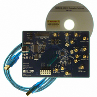
Eval Board
Manufacturer
Analog Devices Inc
Series
AgileRF™r
Specifications of AD9912/PCBZ
Kit Features
Flexible System Clock I/P Accepts Crystal
Supported Devices
AD9912
Tool / Board Applications
Direct Digital Synthesizer
Development Tool Type
Hardware - Eval/Demo Board
Mcu Supported Families
AD9912
Main Purpose
Timing, Direct Digital Synthesis (DDS)
Embedded
No
Utilized Ic / Part
AD9912
Primary Attributes
14-Bit DAC, 48-Bit Tuning Word Width
Secondary Attributes
1GHz, Graphical User Interface
Lead Free Status / RoHS Status
Lead free / RoHS Compliant
Lead Free Status / RoHS Status
Lead free / RoHS Compliant, Lead free / RoHS Compliant


AD9912/PCBZ
USING AN OSCILLATOR FOR THE SYSTEM CLOCK
1.
2.
3.
•
•
•
Solder the 5 mm × 7 mm oscillator to X4.
R101, R102, and R103 may need to be adjusted or removed
depending on the oscillator output type. Refer to the
evaluation board schematic on the CD-ROM for details.
Install the appropriate system clock PLL loop filter, and
remove the 1 kΩ pull-down resistor on the LF pin. Refer to
the evaluation board schematic on the supplied CD-ROM
for details.
HSTL driver: put a 50 Ω terminator on OUTB (J2),
and connect OUT (J1) to a spectrum analyzer.
Connect DUT FILTER OUT (J5) to FDBK IN (J6).
Note that this step is not necessary if R20 (near J5)
and R18 (near FDBK IN/J6) are stuffed. Enable the
HSTL driver in the evaluation software.
Filtered DAC output: remove R13, and put a 0 Ω
resistor across R12. Remove R20. Connect a spectrum
analyzer to DUT FILTER OUT (J5).
Unfiltered DAC output: remove R12, and put a 0 Ω
resistor across R13. Connect a spectrum analyzer to
DUT OUT/FILTER IN (J4).
Rev. 0 | Page 4 of 12
USING A CRYSTAL FOR THE SYSTEM CLOCK
1.
2.
3.
4.
5.
6.
USING AN EXTERNAL RECONSTRUCTION FILTER
1.
2.
Remove C100, C101, and Transformer T5.
Solder crystal to X2 or X3, depending on size.
Install R104 and R105. 0 Ω is a recommended starting
point, but the user may need to experiment with higher
values if the crystal is being overdriven.
Refer to the evaluation board schematic on the supplied
CD-ROM for recommended values of C84, C21, and L4.
Change JMP1 to straddle the center pin and GND.
Install the appropriate system clock PLL loop filter, and
remove the 1 kΩ pull-down resistor on the LF pin. Refer to
the evaluation board schematic on the supplied CD-ROM
for details.
Install a 0 Ω resistor at R13, and remove R20 and R18.
Connect the single-ended reconstruction filter to J4 and J6.
Related parts for AD9912/PCBZ
Image
Part Number
Description
Manufacturer
Datasheet
Request
R


Part Number:
Description:
±1.7g Dual-Axis IMEMS Accelerometer Evaluation Board
Manufacturer:
Analog Devices Inc
Datasheet:

Part Number:
Description:
Inertial Sensor Evaluation System
Manufacturer:
Analog Devices Inc
Datasheet:
Part Number:
Description:
Manufacturer:
Analog Devices Inc
Datasheet:
Part Number:
Description:
Manufacturer:
Analog Devices Inc
Datasheet:
Part Number:
Description:
Manufacturer:
Analog Devices Inc
Datasheet:
Part Number:
Description:
Manufacturer:
Analog Devices Inc
Datasheet:
Part Number:
Description:
Manufacturer:
Analog Devices Inc
Datasheet:
Part Number:
Description:
Manufacturer:
Analog Devices Inc
Datasheet:
Part Number:
Description:
Manufacturer:
Analog Devices Inc
Datasheet:
Part Number:
Description:
Manufacturer:
Analog Devices Inc
Datasheet:
Part Number:
Description:
Manufacturer:
Analog Devices Inc
Datasheet:
Part Number:
Description:
Manufacturer:
Analog Devices Inc
Datasheet: