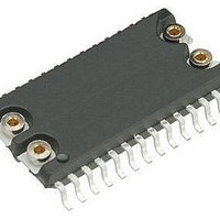
M41T256YMT7 STMicroelectronics, M41T256YMT7 Datasheet - Page 9

M41T256YMT7
Manufacturer Part Number
M41T256YMT7
Description
Real Time Clock Serial 256K (32Kx8)
Manufacturer
STMicroelectronics
Datasheet
1.M41T256YMT7.pdf
(30 pages)
Specifications of M41T256YMT7
Function
Clock, Calendar
Rtc Memory Size
32768 B
Supply Voltage (max)
5.5 V
Supply Voltage (min)
4.5 V
Maximum Operating Temperature
+ 70 C
Minimum Operating Temperature
- 25 C
Mounting Style
SMD/SMT
Rtc Bus Interface
Serial
Package / Case
SO-44
Time Format
HH:MM:SS:hh
Lead Free Status / RoHS Status
Lead free / RoHS Compliant
Available stocks
Company
Part Number
Manufacturer
Quantity
Price
Company:
Part Number:
M41T256YMT7F
Manufacturer:
STMicroelectronics
Quantity:
135
2
2.1
2.1.1
Operating modes
The M41T256Y clock operates as a slave device on the serial bus. Access is obtained by
implementing a start condition followed by the correct slave address (D0h). The 256K bytes
contained in the device can then be accessed sequentially in the following order:
0-7FEF = General purpose RAM
7FF0-7FF6 = Reserved
7FF7h = Tenths/hundredths register
7FF8h = Control register
7FF9h = Seconds register
7FFAh = Minutes register
7FFBh = Hour register
7FFCh = Tamper/day register
7FFDh = Date register
7FFEh = Month register
7FFFh = Year register
The M41T256Y clock continually monitors V
V
address counter. Inputs to the device will not be recognized at this time to prevent
erroneous data from being written to the device from an out-of-tolerance system. When V
falls below V
an ultra low current mode of operation to conserve battery life. As system power returns and
V
external V
For more information on Battery Storage Life refer to Application Note AN1012.
2-wire bus characteristics
The bus is intended for communication between different ICs. It consists of two lines: a
bidirectional data signal (SDA) and a clock signal (SCL). Both the SDA and SCL lines must
be connected to a positive supply voltage via a pull-up resistor.
The following protocol has been defined:
●
●
●
Accordingly, the following bus conditions have been defined:
Bus not busy
Both data and clock lines remain High.
CC
CC
fall below V
rises above V
Data transfer may be initiated only when the bus is not busy.
During data transfer, the data line must remain stable whenever the clock line is high.
Changes in the data line, while the clock line is high, will be interpreted as control
signals.
CC
SO
. Write protection continues until V
, the device automatically switches over to the battery and powers down into
PFD
SO
, the device terminates an access in progress and resets the device
, the battery is disconnected, and the power supply is switched to
CC
CC
for an out-of tolerance condition. Should
reaches V
PFD
plus t
REC
.
9/30
CC


