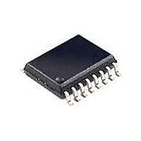
DS3231M+ Maxim Integrated Products, DS3231M+ Datasheet - Page 16

DS3231M+
Manufacturer Part Number
DS3231M+
Description
Real Time Clock +/-5ppm, I2C Real-Ti me Clock with Intern
Manufacturer
Maxim Integrated Products
Datasheet
1.DS3231M.pdf
(20 pages)
Specifications of DS3231M+
Function
Clock, Calendar, Alarm
Supply Voltage (max)
5.5 V
Supply Voltage (min)
2.3 V
Maximum Operating Temperature
+ 85 C
Minimum Operating Temperature
- 40 C
Mounting Style
SMD/SMT
Rtc Bus Interface
I2C
Supply Current
300 uA
Package / Case
SOIC-16
Time Format
HH:MM:SS
Date Format
YY-MM-DD
Lead Free Status / RoHS Status
Lead free / RoHS Compliant
The device’s slave address byte is D0h. The first byte
sent to the device includes the device identifier, device
address, and the R/W bit (Figure 8). The device address
sent by the I 2 C master must match the address assigned
to the device.
The following terminology is commonly used to describe
I 2 C data transfers.
Figure 8. I
±5ppm, I
16
Temperature Register (Upper Byte = 11h)
Temperature Register (Lower Byte = 12h)
Temperature is represented as a 10-bit code with a resolution of 0.25°C and is accessible at location 11h and 12h. The tem-
perature is encoded in two’s complement format. The upper 8 bits, the integer portion, are at location 11h and the lower 2 bits,
the fractional portion, are at location 12h. For example, 00011001 01b = +25.25°C. Upon power reset, the registers are set to
a default temperature of 0°C and the controller starts a temperature conversion. The temperature is read upon initial applica-
tion of V
Temperature registers are also updated after each user-initiated conversion and are read only.
Master Device: The master device controls the slave
devices on the bus. The master device generates
SCL clock pulses and START and STOP conditions.
Slave Devices: Slave devices send and receive data
at the master’s request.
DATA
BIT 7
SIGN
BIT 7
0
0
CC
2
C Slave Address Byte
MSB
or I
1
2
IDENTIFIER
C access on V
I
1
DEVICE
2
C Serial Port Operation
DATA
DATA
BIT 6
BIT 6
0
2
0
0
C Real-Time Clock
1
BAT
0
and once every second afterwards with V
I
2
0
C Slave Address
DATA
BIT 5
BIT 5
I
0
0
0
2
0
C Definitions
WRITE BIT
READ/
LSB
R/W
DATA
BIT 4
BIT 4
0
0
0
DATA
BIT 3
BIT 3
Temperature Registers (11h-12h)
0
0
0
Bus Idle or Not Busy: Time between STOP and
START conditions when both SDA and SCL are
inactive and in their logic-high states. When the bus
is idle, it often initiates a low-power mode for slave
devices.
START Condition: A START condition is generated
by the master to initiate a new data transfer with a
slave. Transitioning SDA from high to low while SCL
remains high generates a START condition. See
Figure 1 for applicable timing.
STOP Condition: A STOP condition is generated
by the master to end a data transfer with a slave.
Transitioning SDA from low to high while SCL remains
high generates a STOP condition. See Figure 1 for
applicable timing.
Repeated START Condition: The master can use
a repeated START condition at the end of one data
transfer to indicate that it immediately initiates a new
data transfer following the current one. Repeated
STARTs are commonly used during read operations
to identify a specific memory address to begin a data
transfer. A repeated START condition is issued iden-
tically to a normal START condition. See Figure 1 for
applicable timing.
CC
power or once every 10s with V
DATA
BIT 2
BIT 2
0
0
0
DATA
BIT 1
BIT 1
0
0
0
BAT
power. The
DATA
BIT 0
BIT 0
0
0
0


