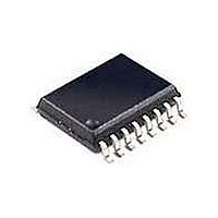
DS3231M+ Maxim Integrated Products, DS3231M+ Datasheet - Page 10

DS3231M+
Manufacturer Part Number
DS3231M+
Description
Real Time Clock +/-5ppm, I2C Real-Ti me Clock with Intern
Manufacturer
Maxim Integrated Products
Datasheet
1.DS3231M.pdf
(20 pages)
Specifications of DS3231M+
Function
Clock, Calendar, Alarm
Supply Voltage (max)
5.5 V
Supply Voltage (min)
2.3 V
Maximum Operating Temperature
+ 85 C
Minimum Operating Temperature
- 40 C
Mounting Style
SMD/SMT
Rtc Bus Interface
I2C
Supply Current
300 uA
Package / Case
SOIC-16
Time Format
HH:MM:SS
Date Format
YY-MM-DD
Lead Free Status / RoHS Status
Lead free / RoHS Compliant
±5ppm, I
by V
device is powered by V
When V
low). When V
temperature conversions are executed once per second.
When V
perature conversions are executed once every 10s.
To preserve the battery, the first time V
to the device the oscillator does not start up until V
exceeds V
the device. Typical oscillator startup time is less than
1s. Approximately 2s after V
I
measurement and applies the calculated correction to
the oscillator. Once the oscillator is running, it continues
to run as long as a valid power source is available (V
or V
perature and correct the oscillator frequency. On the first
application of V
valid I
date registers are reset to 01/01/00 01 00:00:00 (MM/DD/
YY DOW HH:MM:SS).
There are several modes of operation that affect the
amount of V
is powered by V
the active battery current I
serial interface is inactive, the timekeeping current I
(which includes the averaged temperature-conversion
current I
current I
able to support the periodic higher current pulse and
still maintain a valid voltage level. The data-retention
current I
the oscillator is stopped (EOSC = 1). This mode can be
used to minimize battery requirements for periods when
maintaining time and date information is not necessary,
e.g., while the end system is waiting to be shipped to a
customer.
The device provides for a pushbutton switch to be con-
nected to the RST input/output pin. When the device is
not in a reset cycle, it continuously monitors RST for a
low-going edge. If an edge transition is detected, the
device debounces the switch by pulling RST low. After
the internal timer has expired (PB
tinues to monitor the RST line. If the line is still low, the
device continuously monitors the line looking for a rising
10
2
C address is written, the device makes a temperature
BAT
CC
2
. If V
C address is written to the device, the time and
BAT
), and the device continues to measure the tem-
CC
BATDR
BATTC
BATTC
PF
CC
is the presently selected power source, tem-
< V
BAT
CC
or until a valid I
is less than V
) is used. The temperature-conversion
is the current drawn by the device when
CC
PF
is specified since the system must be
is the presently selected power source,
current that is drawn. While the device
BAT
, the RST output is asserted (active
power, or (if V
2
Pushbutton Reset Function
and the serial interface is active,
BAT
C Real-Time Clock
PF
(see Table 1).
BATA
CC
and is less than V
2
C address is written to
BAT
is applied, or a valid
DB
is drawn. When the
), the device con-
powered) when a
V
BAT
BAT
Operation
is applied
BAT
BATT
, the
CC
CC
edge. Upon detecting release, the device forces RST
low and holds it low for t
a power-fail condition. When V
internal power-fail signal is generated, which forces RST
low. When V
low for approximately 250ms (t
supply to stabilize. If the oscillator is not running when
V
ately goes high. Assertion of the RST output, whether by
pushbutton or power-fail detection, does not affect the
device’s internal operation. RST output operation and
pushbutton monitoring are only available if V
is available.
With the 1Hz source from the temperature-compensated
oscillator, the RTC provides seconds, minutes, hours,
day, date, month, and year information. The date at the
end of the month is automatically adjusted for months
with fewer than 31 days, including corrections for leap
year. The clock operates in either the 24-hour or the
12-hour format with an AM/PM indicator. The clock pro-
vides two programmable time-of-day alarms. INT/SQW
can be enabled to generate either an interrupt due to an
alarm condition or a 1Hz square wave. This selection is
controlled by the INTCN bit in the Control register.
The I
V
to the device resets because of a loss of V
event, it is possible that the microcontroller and device’s
I
e.g., the microcontroller resets while reading data from
the device. When the microcontroller resets, the device’s
I
gling SCL until SDA is observed to be at a high level. At
that point the microcontroller should pull SDA low while
SCL is high, generating a START condition.
Table 2 shows the address map for the device’s time-
keeping registers. During a multibyte access, when the
address pointer reaches the end of the register space
(12h), it wraps around to location 00h. On an I
or address pointer incrementing to location 00h, the cur-
rent time is transferred to a second set of registers. The
time information is read from these secondary registers,
while the clock can continue to run. This eliminates the
need to reread the registers in case the main registers
update during a read.
2
2
CC
BAT
C communications could become unsynchronized,
C interface can be placed into a known state by tog-
2
is applied, t
is at a valid level. If a microcontroller connected
C interface is accessible whenever either V
CC
returns to a level above V
REC
is bypassed and RST immedi-
RST
Real-Time Clock (RTC)
. RST is also used to indicate
CC
REC
is lower than V
) to allow the power
I
Address Map
2
PF
C Interface
, RST is held
CC
2
CC
C START
or other
PF
power
CC
, an
or


