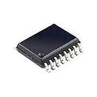
DS3231M+ Maxim Integrated Products, DS3231M+ Datasheet - Page 12

DS3231M+
Manufacturer Part Number
DS3231M+
Description
Real Time Clock +/-5ppm, I2C Real-Ti me Clock with Intern
Manufacturer
Maxim Integrated Products
Datasheet
1.DS3231M.pdf
(20 pages)
Specifications of DS3231M+
Function
Clock, Calendar, Alarm
Supply Voltage (max)
5.5 V
Supply Voltage (min)
2.3 V
Maximum Operating Temperature
+ 85 C
Minimum Operating Temperature
- 40 C
Mounting Style
SMD/SMT
Rtc Bus Interface
I2C
Supply Current
300 uA
Package / Case
SOIC-16
Time Format
HH:MM:SS
Date Format
YY-MM-DD
Lead Free Status / RoHS Status
Lead free / RoHS Compliant
Table 3. Alarm Mask Bits
±5ppm, I
to 00. The day-of-week register increments at midnight.
Values that correspond to the day of week are user-
defined but must be sequential (i.e., if 1 equals Sunday,
then 2 equals Monday, and so on). Illogical time and
date entries result in undefined operation. When reading
or writing the time and date registers, secondary buffers
are used to prevent errors when the internal registers
update. When reading the time and date registers, the
secondary buffers are synchronized to the internal reg-
isters on any I
rolls over to zero. The time information is read from these
secondary registers, while the clock continues to run.
This eliminates the need to reread the registers in case
the main registers update during a read. The countdown
chain is reset whenever the seconds register is writ-
ten. Write transfers occur on the acknowledge from the
device. Once the countdown chain is reset, to avoid roll-
over issues the remaining time and date registers must
be written within 1s.
The device contains two time-of-day/date alarms. Alarm
1 can be set by writing to registers 07h–0Ah. Alarm
2 can be set by writing to registers 0Bh–0Dh. See
Table 2. The alarms can be programmed (by the alarm
12
DY/DT
DY/DT
X
X
X
X
X
X
X
0
1
0
1
A1M4
2
ALARM 1 REGISTER MASK BITS (BIT 7)
ALARM 2 REGISTER MASK BITS (BIT 7)
C START and when the register pointer
1
1
1
1
0
0
A2M4
1
1
1
0
0
2
C Real-Time Clock
A1M3
1
1
1
0
0
0
A2M3
1
1
0
0
0
A1M2
1
1
0
0
0
0
Alarms
A2M2
A1M1
1
0
0
0
0
1
0
0
0
0
0
Alarm once a second
Alarm when seconds match
Alarm when minutes and seconds match
Alarm when hours, minutes, and seconds match
Alarm when date, hours, minutes, and seconds match
Alarm when day, hours, minutes, and seconds match
Alarm once per minute (00 seconds of every minute)
Alarm when minutes match
Alarm when hours and minutes match
Alarm when date, hours, and minutes match
Alarm when day, hours, and minutes match
enable and INTCN bits in the Control register) to acti-
vate the INT/SQW output on an alarm match condition.
Bit 7 of each of the time-of-day/date alarm registers are
mask bits (Table 2). When all the mask bits for each
alarm are logic 0, an alarm only occurs when the values
in the timekeeping registers match the corresponding
values stored in the time-of-day/date alarm registers.
The alarms can also be programmed to repeat every
second, minute, hour, day, or date. Table 3 shows the
possible settings. Configurations not listed in the table
result in illogical operation. The DY/DT bits (bit 6 of the
alarm day/date registers) control whether the alarm
value stored in bits 0–5 of that register reflects the day
of the week or the date of the month. If DY/DT is written
to logic 0, the alarm is the result of a match with date of
the month. If DY/DT is written to logic 1, the alarm is the
result of a match with day of the week. When the RTC
register values match alarm register settings, the cor-
responding alarm flag A1F or A2F bit is set to logic 1. If
the corresponding alarm interrupt enable A1IE or A2IE
bit is also set to logic 1, the alarm condition activates
the INT/SQW signal if the INTCN bit is set to logic 1. The
match is tested on the once-per-second update of the
time and date registers.
ALARM RATE
ALARM RATE


