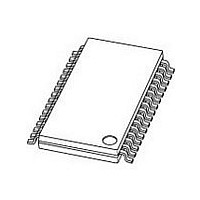
TDA8932BTW NXP Semiconductors, TDA8932BTW Datasheet - Page 26

TDA8932BTW
Manufacturer Part Number
TDA8932BTW
Description
Audio Amplifiers 2X15W BTL CLASS D AMP+VOLCTRL
Manufacturer
NXP Semiconductors
Datasheet
1.TDA8932BTW.pdf
(48 pages)
Specifications of TDA8932BTW
Product
Class-D
Output Power
55 W
Available Set Gain
36 dB
Common Mode Rejection Ratio (min)
75 dB
Thd Plus Noise
0.007 %
Operating Supply Voltage
22 V
Supply Current
0.6 mA
Maximum Power Dissipation
5000 mW
Maximum Operating Temperature
+ 85 C
Mounting Style
SMD/SMT
Audio Load Resistance
8 Ohms
Dual Supply Voltage
+/- 11 V
Input Signal Type
Differential
Minimum Operating Temperature
- 40 C
Output Signal Type
Differential, Single
Supply Type
Single or Dual
Supply Voltage (max)
36 V
Supply Voltage (min)
10 V
Output Type
1-Channel Mono or 2-Channel Stereo
Package / Case
HTSSOP-32
Operational Class
Class-D
Audio Amplifier Output Configuration
1-Channel Mono/2-Channel Stereo
Audio Amplifier Function
Speaker
Total Harmonic Distortion
0.007@8Ohm@1W%
Single Supply Voltage (typ)
22V
Dual Supply Voltage (typ)
±11V
Supply Current (max)
0.195@22VmA
Power Supply Requirement
Single/Dual
Power Dissipation
5W
Rail/rail I/o Type
No
Single Supply Voltage (min)
10V
Single Supply Voltage (max)
36V
Dual Supply Voltage (min)
±5V
Dual Supply Voltage (max)
±18V
Operating Temp Range
-40C to 85C
Operating Temperature Classification
Industrial
Mounting
Surface Mount
Pin Count
32
Package Type
HTSSOP EP
Lead Free Status / RoHS Status
Lead free / RoHS Compliant
Other names
TDA8932BTW/N2
Available stocks
Company
Part Number
Manufacturer
Quantity
Price
Part Number:
TDA8932BTW
Manufacturer:
PHILIPS/飞利浦
Quantity:
20 000
Company:
Part Number:
TDA8932BTW/N2
Manufacturer:
NXP
Quantity:
200
Part Number:
TDA8932BTW/N2
Manufacturer:
NXP/恩智浦
Quantity:
20 000
Company:
Part Number:
TDA8932BTW/N2118
Manufacturer:
NXP Semiconductors
Quantity:
1 876
NXP Semiconductors
TDA8932B_4
Product data sheet
14.6 Device synchronization
14.7 Thermal behavior (printed-circuit board considerations)
Where:
Example:
Substituting R1 = R2 = 4.7 k , Z
results in a gain of G
If two or more TDA8932B devices are used in one application it is recommended that all
devices are synchronized running at the same switching frequency to avoid beat tones.
Synchronization can be realized by connecting all OSCIO pins together and configuring
one of the TDA8932B devices as master, while the other TDA8932B devices are
configured as slaves (see
A device is configured as master when connecting a resistor between pins OSCREF and
V
oscillator output for synchronization. The OSCREF pins of the slave devices should be
shorted to V
The TDA8932B is available in two different thermally enhanced packages:
The SO32 package has special thermal corner-leads, increasing the power capability
(reducing the overall R
and 32) should be attached to a copper plane. The SO32 package is very suitable for
applications with limited space for a thermal plane (in a single layer PCB design).
R
Fig 11. Master slave concept in two chip application
SSD(HW)
EQ
R
R3 = parallel resistor ( )
Z
TDA8932BT in a SO32 (SOT287-1) package for reflow and wave solder process
TDA8932BTW in an HTSSOP32 (SOT549-1) package for reflow solder process only
i
EQ
= internal input impedance ( )
=
= equivalent resistance ( )
----------------- -
R3
R3
setting the carrier frequency. Pin OSCIO of the master is then configured as an
+
SSD(HW)
Z
Z
i
i
100 nF
C osc
configuring pin OSCIO as an input.
master
v(tot)
Rev. 04 — 18 December 2008
OSCREF V
th(j-a)
= 26.3 dB.
Figure
R osc
39 k
. To benefit from the corner leads pins V
TDA8932B
SSD(HW)
IC1
i
11).
= 100 k and R3 = 22 k in
OSCIO
slave
OSCIO
TDA8932B
V
SSD(HW)
IC2
Equation 8
Class-D audio amplifier
OSCREF
SSD(HW)
001aaf600
TDA8932B
© NXP B.V. 2008. All rights reserved.
and
(pins 1, 16, 17
Equation 9
26 of 48
(9)


