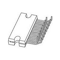
TDA8566Q/N2C NXP Semiconductors, TDA8566Q/N2C Datasheet - Page 7

TDA8566Q/N2C
Manufacturer Part Number
TDA8566Q/N2C
Description
Audio Amplifiers 2X25W BTL STEREO RADIO PWR AMP
Manufacturer
NXP Semiconductors
Datasheet
1.TDA8566QN2C.pdf
(21 pages)
Specifications of TDA8566Q/N2C
Product
Class-B
Output Power
55 W
Available Set Gain
26 dB
Common Mode Rejection Ratio (min)
60 dB
Thd Plus Noise
0.05 %
Operating Supply Voltage
14.4 V
Maximum Power Dissipation
60000 mW
Maximum Operating Temperature
+ 85 C
Mounting Style
Through Hole
Audio Load Resistance
4 Ohms
Input Signal Type
Differential
Minimum Operating Temperature
- 40 C
Output Signal Type
Differential
Supply Type
Single
Supply Voltage (max)
18 V
Supply Voltage (min)
6 V
Output Type
2-Channel Stereo
Package / Case
DBS17P
Operational Class
Class-B
Audio Amplifier Output Configuration
2-Channel Stereo
Output Power (typ)
55x2@2OhmW
Audio Amplifier Function
Speaker
Total Harmonic Distortion
0.05@4Ohm@1W%
Single Supply Voltage (typ)
14.4V
Dual Supply Voltage (typ)
Not RequiredV
Power Supply Requirement
Single
Power Dissipation
60W
Rail/rail I/o Type
No
Single Supply Voltage (min)
6V
Single Supply Voltage (max)
18V
Dual Supply Voltage (min)
Not RequiredV
Dual Supply Voltage (max)
Not RequiredV
Operating Temp Range
-40C to 85C
Operating Temperature Classification
Industrial
Mounting
Through Hole
Pin Count
17
Package Type
DBS17P
Lead Free Status / RoHS Status
Lead free / RoHS Compliant
Other names
TDA8566Q/N2C,112
NXP Semiconductors
TDA8566_6
Product data sheet
7.3 Short-circuit diagnostic (pin DIAG)
7.4 Temperature pre-warning (pin DIAG)
7.5 Open-collector diagnostic outputs
When a short-circuit occurs at one or more outputs to ground or to the supply voltage, the
output stages are switched off until the short-circuit is removed and the device is switched
on again (with a delay of approximately 20 ms after the removal of the short-circuit).
During this short-circuit condition, pin DIAG is continuously LOW.
When a short-circuit occurs across the load of one or both channels, the output stages are
switched off for approximately 20 ms. After that time the load condition is checked during
approximately 50 s to see whether the short-circuit is still present. Due to this duty cycle
of 50 s/20 ms the average current consumption during the short-circuit condition is very
low (approximately 40 mA). During this condition, pin DIAG is LOW for 20 ms and HIGH
for 50 s; see
When the virtual junction temperature (T
continuously LOW.
Pins DIAG and CLIP are open-collector outputs, therefore more devices can be tied
together. Pins DIAG and CLIP can also be tied together. An external pull-up resistor is
required.
Fig 5. Clip detection waveforms
Fig 6. Short-circuit diagnostic timing diagram
current
output
V
stage
DIAG
(V)
in
Figure
short-circuit over the load
6. The power dissipation in any short-circuit condition is very low.
Rev. 06 — 15 October 2007
V
V
(V)
CLIP
(V)
O
0
0
2
40 W/2
vj
50 s
) reaches 145 C, pin DIAG will become
stereo BTL car radio power amplifier
20 ms
mgu357
t (s)
TDA8566
© NXP B.V. 2007. All rights reserved.
t (s)
t (s)
mgu360
7 of 21


