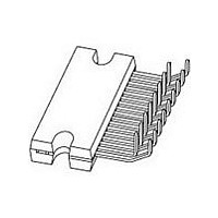
TDA8566Q/N2C NXP Semiconductors, TDA8566Q/N2C Datasheet - Page 2

TDA8566Q/N2C
Manufacturer Part Number
TDA8566Q/N2C
Description
Audio Amplifiers 2X25W BTL STEREO RADIO PWR AMP
Manufacturer
NXP Semiconductors
Datasheet
1.TDA8566QN2C.pdf
(21 pages)
Specifications of TDA8566Q/N2C
Product
Class-B
Output Power
55 W
Available Set Gain
26 dB
Common Mode Rejection Ratio (min)
60 dB
Thd Plus Noise
0.05 %
Operating Supply Voltage
14.4 V
Maximum Power Dissipation
60000 mW
Maximum Operating Temperature
+ 85 C
Mounting Style
Through Hole
Audio Load Resistance
4 Ohms
Input Signal Type
Differential
Minimum Operating Temperature
- 40 C
Output Signal Type
Differential
Supply Type
Single
Supply Voltage (max)
18 V
Supply Voltage (min)
6 V
Output Type
2-Channel Stereo
Package / Case
DBS17P
Operational Class
Class-B
Audio Amplifier Output Configuration
2-Channel Stereo
Output Power (typ)
55x2@2OhmW
Audio Amplifier Function
Speaker
Total Harmonic Distortion
0.05@4Ohm@1W%
Single Supply Voltage (typ)
14.4V
Dual Supply Voltage (typ)
Not RequiredV
Power Supply Requirement
Single
Power Dissipation
60W
Rail/rail I/o Type
No
Single Supply Voltage (min)
6V
Single Supply Voltage (max)
18V
Dual Supply Voltage (min)
Not RequiredV
Dual Supply Voltage (max)
Not RequiredV
Operating Temp Range
-40C to 85C
Operating Temperature Classification
Industrial
Mounting
Through Hole
Pin Count
17
Package Type
DBS17P
Lead Free Status / RoHS Status
Lead free / RoHS Compliant
Other names
TDA8566Q/N2C,112
NXP Semiconductors
3. Quick reference data
4. Ordering information
Table 2.
TDA8566_6
Product data sheet
Type number Package
TDA8566TH
TDA8566TH1
TDA8566Q
Ordering information
Name
HSOP20
HSOP24
DBS17P
Table 1.
V
specified.
[1]
[2]
[3]
[4]
Symbol Parameter
V
I
I
I
Z
P
SVRR
CMRR
G
V
ORM
q
stb
P
i
cs
P
o
n(o)
v
= 14.4 V; T
Description
plastic, heatsink small outline package; 20 leads; low stand-off height
plastic, heatsink small outline package; 24 leads; low stand-off height
plastic DIL-bent-SIL power package; 17 leads (lead length 12 mm)
The circuit is DC adjusted at V
V
Common mode rejection ratio measured at the output (over R
V
Noise measured in a bandwidth of 20 Hz to 20 kHz.
ripple
common
= V
supply voltage
repetitive peak output
current
quiescent current
standby current
input impedance
output power
supply voltage ripple
rejection
channel separation
common mode rejection
ratio
closed loop voltage gain
noise output voltage
Quick reference data
ripple(max)
3.5 V (RMS); f
amb
= 25 C; f
= 2 V (p-p); R
Rev. 06 — 15 October 2007
i
= 100 Hz to 10 kHz; R
i
= 1 kHz; measured in test circuit of
P
= 6 V to 18 V and AC operating at V
s
= 0 .
Conditions
R
differential
R
R
operating
P
R
operating; R
o
L
L
L
s
2
= 25 W; R
= 0
=
= 4 ; THD = 10 %
= 2 ; THD = 10 %
40 W/2
s
= 0 .
s
s
= 0
= 10 k
stereo BTL car radio power amplifier
L
) with both inputs tied together;
[1]
[2]
[3]
[4]
Figure
P
Min
6
-
-
-
100
21
33
50
45
60
25
-
= 8.5 V to 18 V.
9; unless otherwise
Typ
14.4
-
115
0.1
120
25
40
60
50
75
26
85
TDA8566
© NXP B.V. 2007. All rights reserved.
Max
18
7.5
180
10
150
-
-
-
-
-
27
120
Version
SOT418-3
SOT566-3
SOT243-1
Unit
V
A
mA
k
W
W
dB
dB
dB
dB
2 of 21
A
V


