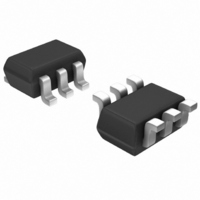
SI1499DH-T1-E3 Vishay, SI1499DH-T1-E3 Datasheet - Page 7
SI1499DH-T1-E3
Manufacturer Part Number
SI1499DH-T1-E3
Description
MOSFET P-CH 8V 1.6A SC70-6
Manufacturer
Vishay
Series
TrenchFET®r
Specifications of SI1499DH-T1-E3
Fet Type
MOSFET P-Channel, Metal Oxide
Fet Feature
Logic Level Gate
Rds On (max) @ Id, Vgs
78 mOhm @ 2A, 4.5V
Drain To Source Voltage (vdss)
8V
Current - Continuous Drain (id) @ 25° C
1.6A
Vgs(th) (max) @ Id
800mV @ 250µA
Gate Charge (qg) @ Vgs
16nC @ 4.5V
Input Capacitance (ciss) @ Vds
650pF @ 4V
Power - Max
2.78W
Mounting Type
Surface Mount
Package / Case
SC-70-6, SC-88, SOT-363
Transistor Polarity
P Channel
Continuous Drain Current Id
1.6A
Drain Source Voltage Vds
-8V
On Resistance Rds(on)
424mohm
Rds(on) Test Voltage Vgs
5V
Threshold Voltage Vgs Typ
-800mV
Configuration
Single Quad Drain
Resistance Drain-source Rds (on)
0.078 Ohms
Drain-source Breakdown Voltage
- 8 V
Gate-source Breakdown Voltage
+/- 5 V
Continuous Drain Current
1.6 A
Power Dissipation
2.5 W
Maximum Operating Temperature
+ 150 C
Mounting Style
SMD/SMT
Minimum Operating Temperature
- 55 C
Lead Free Status / RoHS Status
Lead free / RoHS Compliant
Lead Free Status / RoHS Status
Lead free / RoHS Compliant, Lead free / RoHS Compliant
Other names
SI1499DH-T1-E3TR
Available stocks
Company
Part Number
Manufacturer
Quantity
Price
Company:

Part Number:
SI1499DH-T1-E3
Manufacturer:
Microchip
Quantity:
2 279


INTRODUCTION
The new single 6-pin SC-70 package with a copper leadframe
enables improved on-resistance values and enhanced
thermal performance as compared to the existing 3-pin and
6-pin packages with Alloy 42 leadframes. These devices are
intended for small to medium load applications where a
miniaturized package is required. Devices in this package
come in a range of on-resistance values, in n-channel and
p-channel versions. This technical note discusses pin-outs,
package outlines, pad patterns, evaluation board layout, and
thermal performance for the single-channel version.
BASIC PAD PATTERNS
See Application Note 826, Recommended Minimum Pad
Patterns With Outline Drawing Access for Vishay Siliconix
MOSFETs, (http://www.vishay.com/doc?72286) for the basic
pad layout and dimensions. These pad patterns are sufficient
for the low to medium power applications for which this
package is intended. Increasing the drain pad pattern yields a
reduction in thermal resistance and is a preferred footprint.
The availability of four drain leads rather than the traditional
single drain lead allows a better thermal path from the package
to the PCB and external environment.
PIN-OUT
Figure 1 shows the pin-out description and Pin 1
identification.The pin-out of this device allows the use of four
pins as drain leads, which helps to reduce on-resistance and
junction-to-ambient thermal resistance.
For package dimensions see outline drawing SC-70 (6-Leads)
(http://www.vishay.com/doc?71154)
Document Number: 71334
12-Dec-03
Recommended Pad Pattern and Thermal Performance
Single-Channel LITTLE FOOTR SC-70 6-Pin MOSFET
G
D
D
1
2
3
SC-70 (6-LEADS)
FIGURE 1.
SOT-363
Top View
Copper Leadframe Version
6
5
4
D
D
S
EVALUATION BOARDS
The evaluation board (EVB) measures 0.6 inches by
0.5 inches. The copper pad traces are the same as in Figure 2.
The board allows examination from the outer pins to 6-pin DIP
connections, permitting test sockets to be used in evaluation
testing. See Figure 3.
The thermal performance of the single 6-pin SC-70 has been
measured on the EVB, comparing both the copper and
Alloy 42 leadframes. This test was first conducted on the
traditional Alloy 42 leadframe and was then repeated using the
1-inch
96 (mil)
2
PCB with dual-side copper coating.
71 (mil)
13 (mil)
FIGURE 2.
18 (mil)
0, 0 (mil)
6
1
52 (mil)
26 (mil)
SC-70 (6 leads) Single
Vishay Siliconix
SINGLE SC70-6
5
2
16 (mil)
4
3
www.vishay.com
AN815
26 (mil)
1
Related parts for SI1499DH-T1-E3
Image
Part Number
Description
Manufacturer
Datasheet
Request
R

Part Number:
Description:
P-channel 1.2-v G-s Mosfet
Manufacturer:
Vishay
Datasheet:
Part Number:
Description:
357-036-542-201 CARDEDGE 36POS DL .156 BLK LOPRO
Manufacturer:
Vishay
Datasheet:
Part Number:
Description:
357-036-542-201 CARDEDGE 36POS DL .156 BLK LOPRO
Manufacturer:
Vishay
Datasheet:
Part Number:
Description:
357-036-542-201 CARDEDGE 36POS DL .156 BLK LOPRO
Manufacturer:
Vishay
Datasheet:
Part Number:
Description:
357-036-542-201 CARDEDGE 36POS DL .156 BLK LOPRO
Manufacturer:
Vishay
Datasheet:
Part Number:
Description:
357-036-542-201 CARDEDGE 36POS DL .156 BLK LOPRO
Manufacturer:
Vishay
Datasheet:
Part Number:
Description:
357-036-542-201 CARDEDGE 36POS DL .156 BLK LOPRO
Manufacturer:
Vishay
Datasheet:
Part Number:
Description:
357-036-542-201 CARDEDGE 36POS DL .156 BLK LOPRO
Manufacturer:
Vishay
Datasheet:
Part Number:
Description:
357-036-542-201 CARDEDGE 36POS DL .156 BLK LOPRO
Manufacturer:
Vishay
Datasheet:
Part Number:
Description:
357-036-542-201 CARDEDGE 36POS DL .156 BLK LOPRO
Manufacturer:
Vishay
Datasheet:
Part Number:
Description:
357-036-542-201 CARDEDGE 36POS DL .156 BLK LOPRO
Manufacturer:
Vishay
Datasheet:
Part Number:
Description:
357-036-542-201 CARDEDGE 36POS DL .156 BLK LOPRO
Manufacturer:
Vishay
Datasheet:
Part Number:
Description:
357-036-542-201 CARDEDGE 36POS DL .156 BLK LOPRO
Manufacturer:
Vishay
Datasheet:
Part Number:
Description:
357-036-542-201 CARDEDGE 36POS DL .156 BLK LOPRO
Manufacturer:
Vishay
Datasheet: