NTMD6601NR2G ON Semiconductor, NTMD6601NR2G Datasheet
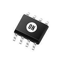
MOSFET N-CH 80V 1.1A 8SOIC

NTMD6601NR2G

Manufacturer Part Number
NTMD6601NR2G
Description
MOSFET N-CH 80V 1.1A 8SOIC
Manufacturer
ON Semiconductor
Datasheet

Specifications of NTMD6601NR2G

Fet Type
2 N-Channel (Dual)
Fet Feature
Logic Level Gate
Rds On (max) @ Id, Vgs
215 mOhm @ 2.2A, 10V
Drain To Source Voltage (vdss)
80V
Current - Continuous Drain (id) @ 25° C
1.1A
Vgs(th) (max) @ Id
3V @ 250µA
Gate Charge (qg) @ Vgs
15nC @ 10V
Input Capacitance (ciss) @ Vds
400pF @ 25V
Power - Max
600mW
Mounting Type
Surface Mount
Package / Case
8-SOIC (3.9mm Width)
Configuration
Dual
Transistor Polarity
N-Channel
Resistance Drain-source Rds (on)
0.19 Ohms
Drain-source Breakdown Voltage
80 V
Gate-source Breakdown Voltage
15 V
Continuous Drain Current
1.4 A
Power Dissipation
1 W
Maximum Operating Temperature
+ 125 C
Mounting Style
SMD/SMT
Gate Charge Qg
5 nC
Minimum Operating Temperature
- 55 C
Lead Free Status / RoHS Status
Lead free / RoHS Compliant
NTMD6601NR2G
Power MOSFET
80 V, 2.2 A, Dual N-Channel, SO-8
Features
Applications
1. Surface-mounted on 2 inch sq FR4 board using 1 inch sq pad size, 1 oz Cu.
2. Surface-mounted on FR4 board using the minimum recommended pad size.
© Semiconductor Components Industries, LLC, 2008
February, 2008 - Rev. 0
MAXIMUM RATINGS
THERMAL RESISTANCE RATINGS
Drain-to-Source Voltage
Gate-to-Source Voltage - Continuous
Continuous Drain
Current R
Power Dissipation
R
Continuous Drain
Current R
Power Dissipation
R
Continuous Drain
Current R
(Note 1)
Pulsed Drain Current
Operating Junction and Storage Temperature
Source Current (Body Diode)
Single Pulse Drain-to-Source Avalanche
Energy T
I
Lead Temperature for Soldering Purposes
(1/8″ from case for 10 s)
Junction-to-Ambient – Steady State (Note 1)
Junction-to-Ambient – t≤ 5 s (Note 1)
Junction-to-FOOT (Drain)
Junction-to-Ambient – Steady State (Note 2)
L
Low R
Low Capacitance to Minimize Driver Losses
Optimized Gate Charge to Minimize Switching Losses
Dual SO-8 Surface Mount Package Saves Board Space
This is a Pb-Free Device
LCD Displays
qJA
qJA
= 7.0 A
(Note 1)
(Note 2)
J
DS(on)
pk
qJA
qJA
qJA
= 25C, V
, L = 1.0 mH, R
(Note 1)
(Note 2)
t < 5 s
to Minimize Conduction Losses
Rating
Rating
DD
= 50 V, V
(T
Steady
G
State
J
= 25 W
= 25°C unless otherwise stated)
T
t
A
p
GS
= 10 ms
= 25°C,
T
T
= 10 V,
T
T
T
T
T
T
A
A
A
A
A
A
A
A
= 25°C
= 25°C
= 25°C
= 70°C
= 25°C
= 70°C
= 25°C
= 70°C
T
Symbol
Symbol
J
V
R
R
R
EAS
R
V
, T
I
P
P
DSS
DM
T
I
I
I
I
qJA
qJA
qJF
qJA
GS
D
D
D
S
D
D
L
STG
-55 to
Value
+150
Max
±15
260
120
200
1.4
1.2
1.0
1.1
0.9
0.6
2.2
1.7
9.0
1.3
2 5
80
48
40
1
°C/W
Unit
Unit
mJ
°C
°C
W
W
V
V
A
A
A
A
A
†For information on tape and reel specifications,
NTMD6601NR2G
including part orientation and tape sizes, please
refer to our Tape and Reel Packaging Specification
Brochure, BRD8011/D.
V
8
(BR)DSS
80 V
Device
1
ORDERING INFORMATION
6601N = Device Code
A
Y
WW
G
G
http://onsemi.com
245 mW @ 4.5 V
CASE 751
215 mW @ 10 V
STYLE 11
R
= Assembly Location
= Year
= Work Week
= Pb-Free Package
N-Channel
SO-8
(Pb-Free)
DS(on)
Package
SO-8
Publication Order Number:
D
MARKING DIAGRAM
S
& PIN ASSIGNMENT
Max
8
1
2500/Tape & Reel
D1 D1 D2 D2
S1 G1 S2 G2
NTMD6601N/D
AYWW
6601N
Shipping
G
I
D
2.2 A
Max

Related parts for NTMD6601NR2G

NTMD6601NR2G Summary of contents

Page 1

... A S EAS °C T 260 L Symbol Max Unit Device R 120 qJA NTMD6601NR2G R 48 qJA °C qJF †For information on tape and reel specifications, 200 R qJA including part orientation and tape sizes, please refer to our Tape and Reel Packaging Specification Brochure, BRD8011/D. 1 http://onsemi.com ...

Page 2

... BODY - DRAIN DIODE RATINGS (Note 3) Forward Diode Voltage Reverse Recovery Time Charge Time Discharge Time Reverse Recovery Time 3. Pulse Test: pulse width v 300 ms, duty cycle v 2%. 4. Switching characteristics are independent of operating junction temperatures. NTMD6601NR2G (T = 25°C unless otherwise noted) J Symbol Test Condition = 250 mA V ...

Page 3

... T = -55° DRAIN CURRENT (A) D Figure 3. On-Resistance versus Drain Current and Temperature 1.5 1 0.5 0 -50 - JUNCTION TEMPERATURE (°C) J Figure 5. On-Resistance Variation with Temperature NTMD6601NR2G ≥ 3 25° 1.4 1 25°C J 0.25 0.2 0.15 0.1 0. Figure 4. On-Resistance versus Drain Current ...

Page 4

... GATE RESISTANCE (W) G Figure 9. Resistive Switching Time Variation versus Gate Resistance SINGLE PULSE T = 25° LIMIT DS(on) THERMAL LIMIT PACKAGE LIMIT 0.1 0 DRAIN-TO-SOURCE VOLTAGE (V) DS Figure 11. Maximum Rated Forward Biased Safe Operating Area NTMD6601NR2G 25° iss oss Figure 8. Gate-To-Source and Drain-To-Source 2 25°C ...

Page 5

... TYPICAL ELECTRICAL CHARACTERISTICS 0.5 0.2 0.1 0.1 0.05 0.02 0.01 0.01 SINGLE PULSE 0.001 1.0E-05 1.0E-04 1.0E- Figure 14. Diode Reverse Recovery Waveform NTMD6601NR2G Normalized to qja at 10s. 0.0175 W 0.0710 W Chip 0.0154 F 0.0854 F 1.0E-02 1.0E-01 1.0E+00 t, TIME (s) Figure 13. Thermal Response di/ TIME 0. http://onsemi.com 5 0 ...

Page 6

... Opportunity/Affirmative Action Employer. This literature is subject to all applicable copyright laws and is not for resale in any manner. PUBLICATION ORDERING INFORMATION LITERATURE FULFILLMENT:  Literature Distribution Center for ON Semiconductor  P.O. Box 5163, Denver, Colorado 80217 USA  Phone: 303-675-2175 or 800-344-3860 Toll Free USA/Canada  Fax: 303-675-2176 or 800-344-3867 Toll Free USA/Canada  Email: orderlit@onsemi.com NTMD6601NR2G PACKAGE DIMENSIONS SO-8 NB CASE 751-07 ISSUE ...

Related keywords