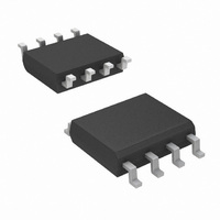
SI4501ADY-T1-E3 Vishay, SI4501ADY-T1-E3 Datasheet

SI4501ADY-T1-E3
Specifications of SI4501ADY-T1-E3
Available stocks
Related parts for SI4501ADY-T1-E3
SI4501ADY-T1-E3 Summary of contents
Page 1
... Top View Ordering Information: Si4501ADY-T1 Si4501ADY-T1-E3 (Lead (Pb)-free) ABSOLUTE MAXIMUM RATINGS T Parameter Drain-Source Voltage Gate-Source Voltage a, b Continuous Drain Current (T = 150 °C) J Pulsed Drain Current Continuous Source Current (Diode Conduction Maximum Power Dissipation Operating Junction and Storage Temperature Range THERMAL RESISTANCE RATINGS ...
Page 2
... Si4501ADY Vishay Siliconix SPECIFICATIONS °C, unless otherwise noted J Parameter Static Gate Threshold Voltage Gate-Body Leakage Zero Gate Voltage Drain Current b On-State Drain Current b Drain-Source On-State Resistance b Forward Transconductance b Diode Forward Voltage a Dynamic Total Gate Charge Gate-Source Charge Gate-Drain Charge Turn-On Delay Time ...
Page 3
... I - Drain Current (A) D On-Resistance vs. Drain Current 8 Total Gate Charge (nC) g Gate Charge Document Number: 71922 S-61005-Rev. B, 12-Jun- Si4501ADY Vishay Siliconix ° ° Gate-to-Source Voltage (V) GS Transfer Characteristics 2000 1600 C iss 1200 800 C oss 400 C rss Drain-to-Source Voltage (V) DS Capacitance 1 1 ...
Page 4
... Si4501ADY Vishay Siliconix N-CHANNEL TYPICAL CHARACTERISTICS 25 °C unless noted 100 T = 150 ° 0.00 0.2 0.4 0 Source-to-Drain Voltage (V) SD Source-Drain Diode Forward Voltage 0 250 µA D 0.2 0.0 - 0.2 - 0.4 - 0 Temperature (°C) J Threshold Voltage www.vishay.com 4 0.10 0.08 0.06 0. °C J 0.02 0.00 0.8 1 ...
Page 5
... Single Pulse 0. Document Number: 71922 S-61005-Rev. B, 12-Jun- Square Wave Pulse Duration (sec) Normalized Thermal Transient Impedance, Junction-to-Ambient - Square Wave Pulse Duration (sec) Normalized Thermal Transient Impedance, Junction-to-Foot Si4501ADY Vishay Siliconix Notes Duty Cycle Per Unit Base = °C/W thJA ( ...
Page 6
... Si4501ADY Vishay Siliconix P-CHANNEL TYPICAL CHARACTERISTICS 25 °C unless noted thru 3 Drain-to-Source Voltage (V) DS Output Characteristics 0. 0. 0.02 0. Drain Current (A) D On-Resistance vs. Drain Current 5 Total Gate Charge (nC) g Gate Charge www.vishay.com 2 1 2000 1600 1200 ° ° 0.0 0.5 1 ...
Page 7
... Limited DS(on °C A Single Pulse 0.1 0.01 0 Drain-to-Source Voltage (V) DS Safe Operating Area Si4501ADY Vishay Siliconix Gate-to-Source Voltage (V) GS On-Resistance vs. Gate-to-Source Voltage 0.001 0.01 0.1 1 Time (sec) Single Pulse Power, Junction-to-Ambient 100 mS ...
Page 8
... Si4501ADY Vishay Siliconix P-CHANNEL TYPICAL CHARACTERISTICS 25 °C unless noted 2 1 Duty Cycle = 0.5 0.2 0.1 0.1 0.05 0.02 Single Pulse 0. Duty Cycle = 0.5 0.2 0.1 0.1 0.05 0.02 Single Pulse 0. Vishay Siliconix maintains worldwide manufacturing capability. Products may be manufactured at one of several qualified locations. Reliability data for Silicon Tech- nology and Package Reliability represent a composite of all qualified locations ...
Page 9
... Information contained herein is intended to provide a product description only. No license, express or implied, by estoppel or otherwise, to any intellectual property rights is granted by this document. Except as provided in Vishay's terms and conditions of sale for such products, Vishay assumes no liability whatsoever, and disclaims any express or implied warranty, relating to sale and/or use of Vishay products including liability or warranties relating to fitness for a particular purpose, merchantability, or infringement of any patent, copyright, or other intellectual property right ...


