STGF20NB60S STMicroelectronics, STGF20NB60S Datasheet
STGF20NB60S
Specifications of STGF20NB60S
Available stocks


Related parts for STGF20NB60S


STGF20NB60S Summary of contents
Page 1
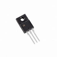
... MOTOR CONTROL Table 2: Order Code PART NUMBER STGF20NB60S August 2005 N-CHANNEL 13A - 600V TO-220FP Figure 1: Package (Max) I CE(sat) C @25°C @100°C < 1 cesat Figure 2: Internal Schematic Diagram MARKING PACKAGE GF20NB60S TO-220FP STGF20NB60S PowerMESH™ IGBT TO-220FP PACKAGING TUBE Rev. 3 1/11 ...
Page 2
... STGF20NB60S Table 3: Absolute Maximum ratings Symbol V Collector-Emitter Voltage (V CES V Emitter-Collector Voltage ECR V Gate-Emitter Voltage GE I Collector Current (continuous Collector Current (continuous Collector Current (pulsed Total Dissipation at T TOT Derating Factor V Insulation withstand voltage AC (t=1sec, Tc=25°C) ISO T Storage Temperature stg T Operating Junction Temperature range ...
Page 3
... J (see Figure 17 480 100 , 125 °C (see Figure 17) Test Conditions V = 480 100 , V = 15V (see Figure 18 480 100 , V =15V,Tj=125° (see Figure 18) STGF20NB60S Min. Typ. Max. Unit 20 S 1820 pF 167 115 Min. Typ. Max. Unit 340 A/µ 320 A/µs Min. ...
Page 4
... STGF20NB60S Figure 3: Output Characteristics Figure 4: Transconductance Figure 5: Collector-Emitter On Voltage vs Col- lector Current 4/11 Figure 6: Transfer Characteristics Figure 7: Normalized Collector-Emitter On Voltage vs Temperature Figure 8: Gate Threshold vs Temperature ...
Page 5
... Figure 9: Normalized Breakdown Voltage vs Temperature Figure 10: Capacitance Variations Figure 11: Switching Losses vs Temperature Figure 12: Gate Charge vs Gate-Emitter Volt- age Figure 13: Switching Losses vs Gate Charge Figure 14: Switching Losses vs Collector Cur- rent STGF20NB60S 5/11 ...
Page 6
... STGF20NB60S Figure 15: Thermal Impedance 6/11 Figure 16: Collector-Emitter Diode Character- istics ...
Page 7
... Figure 17: Test Circuit for Inductive Load Switching Figure 18: Switching Waveforms Figure 19: Gate Charge Test Circuit STGF20NB60S 7/11 ...
Page 8
... STGF20NB60S In order to meet environmental requirements, ST offers these devices in ECOPACK® packages. These packages have a Lead-free second level interconnect . The category of second level interconnect is marked on the package and on the inner box label, in compliance with JEDEC Standard JESD97. The maximum ratings related to soldering conditions are also marked on the inner box label. ECOPACK trademark ...
Page 9
... STGF20NB60S inch MIN. TYP. 0.181 0.106 0.108 0.027 0.039 0.067 0.067 0.204 0.106 0.409 0.630 1.204 0.417 0.141 0.645 0.366 0.126 MAX. 9/11 ...
Page 10
... STGF20NB60S Table 10: Revision History Date Revision 17-Dec-2004 2 05-Aug-2005 3 10/11 Description of Changes New template, no content change Some values changed in table 6 ...
Page 11
... Australia - Belgium - Brazil - Canada - China - Czech Republic - Finland - France - Germany - Hong Kong - India - Israel - Italy - Japan - Malaysia - Malta - Morocco - Singapore - Spain - Sweden - Switzerland - United Kingdom - United States of America All other names are the property of their respective owners © 2005 STMicroelectronics - All Rights Reserved STMicroelectronics group of companies STGF20NB60S 11/11 ...