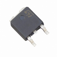
STGD5NB120SZT4 STMicroelectronics, STGD5NB120SZT4 Datasheet - Page 5

STGD5NB120SZT4
Manufacturer Part Number
STGD5NB120SZT4
Description
IGBT N-CHAN 10A 1200V DPAK
Manufacturer
STMicroelectronics
Series
PowerMESH™r
Datasheet
1.STGD5NB120SZ-1.pdf
(15 pages)
Specifications of STGD5NB120SZT4
Voltage - Collector Emitter Breakdown (max)
1200V
Vce(on) (max) @ Vge, Ic
2V @ 15V, 5A
Current - Collector (ic) (max)
10A
Power - Max
75W
Input Type
Standard
Mounting Type
Surface Mount
Package / Case
DPak, TO-252 (2 leads+tab), SC-63
Transistor Type
IGBT
Dc Collector Current
10A
Collector Emitter Voltage Vces
1.2kV
Power Dissipation Pd
75W
Operating Temperature Range
-55°C To +150°C
No. Of Pins
3
Channel Type
N
Configuration
Single
Collector-emitter Voltage
1.2kV
Collector Current (dc) (max)
10A
Gate To Emitter Voltage (max)
±20V
Package Type
DPAK
Pin Count
2 +Tab
Mounting
Surface Mount
Operating Temperature (max)
150C
Operating Temperature Classification
Military
Collector- Emitter Voltage Vceo Max
1200 V
Collector-emitter Saturation Voltage
2 V
Maximum Gate Emitter Voltage
+/- 20 V
Continuous Collector Current At 25 C
10 A
Gate-emitter Leakage Current
+/- 100 nA
Power Dissipation
55 W
Maximum Operating Temperature
+ 150 C
Continuous Collector Current Ic Max
10 A
Minimum Operating Temperature
- 55 C
Mounting Style
SMD/SMT
Collector Emitter Voltage V(br)ceo
1.2kV
Rohs Compliant
Yes
Lead Free Status / RoHS Status
Lead free / RoHS Compliant
Igbt Type
-
Lead Free Status / Rohs Status
Compliant
Other names
497-4352-2
Available stocks
Company
Part Number
Manufacturer
Quantity
Price
Part Number:
STGD5NB120SZT4
Manufacturer:
ST
Quantity:
20 000
STGD5NB120SZ
Table 6.
Table 7.
1.
2. Turn-off losses include also the tail of the collector current
Table 8.
Symbol
(di/dt)
(di/dt)
Symbol
Symbol
t
t
E
E
E
E
t
t
t
t
r
r
offered in a package with a co-pak diode, the co-pack diode is used as external diode. IGBTs & Diode are
at the same temperature (25°C and 125°C)
d
d
d(on)
d(on)
(V
(V
Eon is the turn-on losses when a typical diode is used in the test circuit in
on
on
E
E
I
off
off
(
(
t
t
AS
t
t
t
t
off
off
c
c
r
r
f
f
ts
ts
off
off
(2)
(2)
(1)
(1)
on
on
)
)
)
)
Turn-on delay time
Current rise time
Turn-on current slope
Turn-on delay time
Current rise time
Turn-on current slope
Cross-over time
Off voltage rise time
Turn-off delay time
Current fall time
Cross-over time
Off voltage rise time
Turn-off delay time
Current fall time
Turn-on switching losses
Turn-off switching losses
Total switching losses
Turn-on switching losses
Turn-off switching losses
Total switching losses
Unclamped inductive
switching current
Switching on/off (inductive load)
Switching energy (inductive load)
Functional test
Parameter
Parameter
Parameter
V
R
(see Figure 18)
V
R
T
V
T
V
R
(see Figure 18)
V
R
T
V
R
(see Figure 18)
V
R
T
C
start
CC
CC
CC
C
C
drive
drive
CC
CC
CC
CC
drive
drive
drive
drive
= 125 °C
= 125 °C
= 125 °C
= 960 V, I
= 960 V, I
= 50 V, L = 1.8 mH
= 960 V, I
= 960 V, I
= 960 V, I
= 960 V, I
= 1 kΩ, V
= 1 kΩ, V
= 25 °C, R
= 1 kΩ, V
= 1 kΩ, V
= 1 kΩ, V
= 1 kΩ, V
Test conditions
Test conditions
Test conditions
(see Figure 18)
(see Figure 18)
(see Figure 18)
C
C
C
C
C
C
GE
GE
GE
GE
GE
GE
drive
= 5A
= 5A
= 5A
= 5A
= 5A
= 5A
= 15 V
= 15 V,
= 15 V,
= 15 V
= 15 V
= 15 V,
= 1 kΩ
(see Figure
Electrical characteristics
Min.
Min.
Min.
3.3
11.59
12.68
18). If the IGBT is
Typ.
39.6
12.1
1.13
12.1
Typ.
Typ.
690
170
600
185
2.59
2.64
10.2
2.2
2.2
39
4
5
2
9
Max.
Max.
Max.
A/µs
A/µs
Unit
Unit
Unit
ns
ns
ns
ns
µs
µs
µs
µs
µs
µs
µs
µs
mJ
mJ
mJ
mJ
mJ
mJ
A
5/15


