BAW56S,115 NXP Semiconductors, BAW56S,115 Datasheet - Page 10
BAW56S,115
Manufacturer Part Number
BAW56S,115
Description
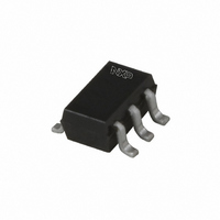
DIODE ARRAY 90V 250MA H-S SOT363
Manufacturer
NXP Semiconductors
Datasheet
1.BAW56S115.pdf
(15 pages)
Specifications of BAW56S,115
Package / Case
SC-70-6, SC-88, SOT-363
Mounting Type
Surface Mount
Speed
Fast Recovery =< 500ns, > 200mA (Io)
Reverse Recovery Time (trr)
4ns
Current - Reverse Leakage @ Vr
500nA @ 80V
Voltage - Forward (vf) (max) @ If
1V @ 50mA
Voltage - Dc Reverse (vr) (max)
90V
Current - Average Rectified (io) (per Diode)
250mA (DC)
Diode Configuration
2 Pair Series Connection
Product
Switching Diodes
Peak Reverse Voltage
90 V
Forward Continuous Current
0.25 A
Max Surge Current
4 A
Configuration
Double Dual Common Anode
Recovery Time
4 ns
Forward Voltage Drop
1.25 V
Maximum Reverse Leakage Current
0.5 uA
Operating Temperature Range
+ 150 C
Maximum Operating Temperature
+ 150 C
Minimum Operating Temperature
- 65 C
Mounting Style
SMD/SMT
Lead Free Status / RoHS Status
Lead free / RoHS Compliant
Lead Free Status / RoHS Status
Lead free / RoHS Compliant, Lead free / RoHS Compliant
Other names
934045730115::BAW56S T/R::BAW56S T/R


NXP Semiconductors
BAV756S_BAW56_SER_5
Product data sheet
Fig 13. Wave soldering footprint BAW56 (SOT23/TO-236AB)
Fig 14. Reflow soldering footprint BAW56M (SOT883/SC-101)
4.60
Reflow soldering is the only recommended soldering method.
4.00
1.20
0.90
R = 0.05 (12 )
0.20
Rev. 05 — 26 November 2007
0.35
0.25
(2 )
(2 )
solder lands
solder paste
2
3.40
2.80
4.50
0.30
0.40
0.50
(2 )
(2 )
(2 )
3
1.20 (2x)
BAV756S; BAW56 series
1
1.30
0.30
solder resist
occupied area
Dimensions in mm
preferred transport direction during soldering
0.30
0.40
0.50
Dimensions in mm
High-speed switching diodes
solder lands
solder resist
occupied area
R = 0.05 (12 )
0.60 0.70 0.80
© NXP B.V. 2007. All rights reserved.
sot023
10 of 15
Related parts for BAW56S,115
Image
Part Number
Description
Manufacturer
Datasheet
Request
R

Part Number:
Description:
Diodes (General Purpose, Power, Switching) DIODE SW TAPE-11
Manufacturer:
NXP Semiconductors

Part Number:
Description:
DIODE ARRAY 90V 250MA H-S SOT363
Manufacturer:
NXP Semiconductors
Datasheet:

Part Number:
Description:
High-speed double diode
Manufacturer:
Philips Semiconductors / NXP Semiconductors

Part Number:
Description:
NXP Semiconductors designed the LPC2420/2460 microcontroller around a 16-bit/32-bitARM7TDMI-S CPU core with real-time debug interfaces that include both JTAG andembedded trace
Manufacturer:
NXP Semiconductors
Datasheet:

Part Number:
Description:
NXP Semiconductors designed the LPC2458 microcontroller around a 16-bit/32-bitARM7TDMI-S CPU core with real-time debug interfaces that include both JTAG andembedded trace
Manufacturer:
NXP Semiconductors
Datasheet:
Part Number:
Description:
NXP Semiconductors designed the LPC2468 microcontroller around a 16-bit/32-bitARM7TDMI-S CPU core with real-time debug interfaces that include both JTAG andembedded trace
Manufacturer:
NXP Semiconductors
Datasheet:
Part Number:
Description:
NXP Semiconductors designed the LPC2470 microcontroller, powered by theARM7TDMI-S core, to be a highly integrated microcontroller for a wide range ofapplications that require advanced communications and high quality graphic displays
Manufacturer:
NXP Semiconductors
Datasheet:
Part Number:
Description:
NXP Semiconductors designed the LPC2478 microcontroller, powered by theARM7TDMI-S core, to be a highly integrated microcontroller for a wide range ofapplications that require advanced communications and high quality graphic displays
Manufacturer:
NXP Semiconductors
Datasheet:
Part Number:
Description:
The Philips Semiconductors XA (eXtended Architecture) family of 16-bit single-chip microcontrollers is powerful enough to easily handle the requirements of high performance embedded applications, yet inexpensive enough to compete in the market for hi
Manufacturer:
NXP Semiconductors
Datasheet:
Part Number:
Description:
The XA-S3 device is a member of Philips Semiconductors? XA(eXtended Architecture) family of high performance 16-bitsingle-chip microcontrollers
Manufacturer:
NXP Semiconductors
Datasheet:

Part Number:
Description:
The NXP BlueStreak LH75401/LH75411 family consists of two low-cost 16/32-bit System-on-Chip (SoC) devices
Manufacturer:
NXP Semiconductors
Datasheet:
Part Number:
Description:
The NXP LPC3130/3131 combine an 180 MHz ARM926EJ-S CPU core, high-speed USB2
Manufacturer:
NXP Semiconductors
Datasheet:
Part Number:
Description:
The NXP LPC3141 combine a 270 MHz ARM926EJ-S CPU core, High-speed USB 2
Manufacturer:
NXP Semiconductors
Part Number:
Description:
The NXP LPC3143 combine a 270 MHz ARM926EJ-S CPU core, High-speed USB 2
Manufacturer:
NXP Semiconductors