PD54003 STMicroelectronics, PD54003 Datasheet
PD54003
Specifications of PD54003
Available stocks


Related parts for PD54003


PD54003 Summary of contents
Page 1
... It is designed for high gain, broad band commercial and industrial applications. It operates common source mode at frequencies GHz. PD54003 boasts the excellent gain, linearity and reliability of ST’s latest LDMOS tech- nology mounted in the first true SMD plastic RF power package, PowerSO-10RF. PD54003’s su- perior linearity performance makes it an ideal so- lution for portable radio ...
Page 2
... PD54003 - PD54003S ELECTRICAL SPECIFICATION (T STATIC (Per Section) Symbol DSS GSS GS( DS(ON ISS OSS RSS GS DYNAMIC Symbol 7 OUT Load DD DQ mismatch ALL PHASE ANGLES PIN CONNECTION GATE SC15200 PD54003 FREQ. MHz IN 480 2.245 - j 0.077 500 1.553 - j 1.251 520 1.993 - j 1.098 2/18 ...
Page 3
... TYPICAL PERFORMANCE Capacitance vs. Drain Voltage 1000 100 VDD, DRAIN VOLTAGE (V) Gate-Source Voltage vs. Case Temperature 1.06 1.04 1.02 1 0.98 0.96 Vds 0.94 0.92 - Tc, CASE TEMPERATURE (°C) Drain Current vs. Gate Voltage iss Crs 100 PD54003 - PD54003S VGS, GATE-SOURCE VOLTAGE (V) Vds = 3/18 ...
Page 4
... PD54003 - PD54003S TYPICAL PERFORMANCE Output Power vs. Input Power 5 4 480 MHz 3 500 MHz 0.1 0.2 Pin, INPUT POWER (W) Drain Efficiency vs. Output Power 80 70 520 MHz Pout, OUTPUT POWER (W) Output Power vs. Bias Current 3.8 3.7 3.6 3.5 3.4 3.3 3.2 3.1 3 2.9 ...
Page 5
... VGS, GATE-SOURCE VOLTAGE (V) Drain Efficiency vs. Supply Voltage 70 480 MHz 60 50 520 MHz 40 30 Pin= 23.3 dBm Idq 480 MHz 520 MHz Pin= 23.3 dBm Vdd= 7 PD54003 - PD54003S 480 MHz 500 MHz 520 MHz Pin= 23.3 dBm Idq VDD, SUPPLY VOLTAGE (V) 10 5/18 ...
Page 6
... PD54003 - PD54003S TYPICAL PERFORMANCE Output Power vs. Input Power 5 500 MHz 480 MHz 0.1 0.2 Pin, INPUT POWER (W) Drain Efficiency vs. Output Power 70 60 500 MHz Pout, OUTPUT POWER (W) Output Power vs. Bias Current 3.5 3.4 3.3 3.2 3.1 3 2.9 2.8 2.7 2.6 0 100 ...
Page 7
... Output Power vs. Gate-Source Voltage 4 480 MHz 3 500 MHz VGS, GATE-SOURCE VOLTAGE (V) Drain Efficiency vs. Supply Volatge 70 480 MHz 60 500 MHz 50 40 Pin= 22 dBm Idq 520 MHz Pin= 22 dBm Vdd= 7 PD54003 - PD54003S 480 MHz 500 MHz 520 MHz VDD, SUPPLY VOLTAGE (V) Pin= 22 dBm Idq 7/18 ...
Page 8
... PD54003 - PD54003S TEST CIRCUIT SCHEMATIC TEST CIRCUIT COMPONENT PART LIST COMPONENT B1,B2 C1,C13 C2,C3,C4,C10,C11,C12 C5 C6,C17 C7,C14 C8,C15 C9,C16 L1 N1, Z6, Z10 Z11 BOARD 8/18 DESCRIPTION SHORT FERRITE BEAD, FAIR RITE PRODUCTS (2743021446) 240 pF, 100 mil CHIP CAPACITOR TRIMMER CAPACITOR 130 pF, 100 mil CHIP CAPACITOR ...
Page 9
... TEST CIRCUIT TEST CIRCUIT PHOTOMASTER 6.4 inches PD54003 - PD54003S 9/18 ...
Page 10
... PD54003 - PD54003S COMMON SOURCE S-PARAMETER (PD54003 7. 50mA FREQ (MHz) 50 0.729 100 0.759 150 0.807 200 0.845 250 0.844 300 0.901 350 0.921 400 0.932 450 0.944 500 0.952 550 0.957 600 0.962 650 0.967 700 0.969 750 0.970 800 0.972 850 ...
Page 11
... COMMON SOURCE S-PARAMETER (PD54003 7. 500mA FREQ (MHz) 50 0.779 100 0.810 150 0.836 200 0.850 250 0.861 300 0.871 350 0.881 400 0.890 450 0.901 500 0.908 550 0.915 600 0.924 650 0.928 700 0.934 750 0.937 800 0.939 850 0.943 900 ...
Page 12
... PD54003 - PD54003S COMMON SOURCE S-PARAMETER (PD54003 7. 1A FREQ (MHz) 50 0.802 -166 100 0.831 -170 150 0.855 -173 200 0.867 -175 250 0.876 -175 300 0.883 -177 350 0.887 -177 400 0.864 -178 450 0.903 -178 500 0.911 -179 550 0.916 -180 600 0 ...
Page 13
... COMMON SOURCE S-PARAMETER (PD54003S 7. 50mA FREQ (MHz) 50 0.749 100 0.760 150 0.799 200 0.837 250 0.869 300 0.893 350 0.913 400 0.932 450 0.941 500 0.949 550 0.961 600 0.965 650 0.969 700 0.970 750 0.974 800 0.977 850 0.979 900 ...
Page 14
... PD54003 - PD54003S COMMON SOURCE S-PARAMETER (PD54003S 7. 500mA FREQ (MHz) 50 0.805 100 0.838 150 0.863 200 0.873 250 0.880 300 0.884 350 0.891 400 0.901 450 0.906 500 0.914 550 0.923 600 0.927 650 0.931 700 0.934 750 0.941 800 0.944 850 ...
Page 15
... COMMON SOURCE S-PARAMETER (PD54003S 7. 1A FREQ (MHz) 50 0.879 -164 100 0.879 -172 150 0.885 -174 200 0.887 -175 250 0.890 -176 300 0.894 -177 350 0.898 -177 400 0.907 -178 450 0.910 -178 500 0.914 -179 550 0.922 -179 600 0.926 ...
Page 16
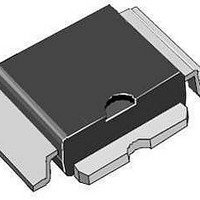
... PD54003 - PD54003S PowerSO-10RF Formed Lead (Gull Wing) MECHANICAL DATA DIM. MIN 3.4 A3 1 5.4 c 0.23 D 9.4 D1 7.4 E 13.85 E1 9.3 E2 7 deg T1 T2 Note (1): Resin protrusions not included (max value: 0.15 mm per side) 16/18 mm TYP. MAX 0.05 0.1 3.5 3.6 1 ...
Page 17
... CRITICAL DIMENSIONS: - Overall width (L) PD54003 - PD54003S Inch MIN. TYP. 0.064 0.065 0.134 0.137 0.046 0.05 0.005 0.007 0.007 0.212 0.217 0.008 0.01 0.370 0.374 ...
Page 18
... PD54003 - PD54003S Information furnished is believed to be accurate and reliable. However, STMicroelectronics assumes no responsibility for the consequences of use of such information nor for any infringement of patents or other rights of third parties which may result from its use. No license is granted by implication or otherwise under any patent or patent rights of STMicroelectronics. Specifications mentioned in this publication are subject to change without notice ...