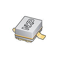
BLF1043 NXP Semiconductors, BLF1043 Datasheet - Page 3

BLF1043
Manufacturer Part Number
BLF1043
Description
RF MOSFET Power RF LDMOS 10W UHF
Manufacturer
NXP Semiconductors
Datasheet
1.BLF1043112.pdf
(12 pages)
Specifications of BLF1043
Minimum Operating Temperature
- 65 C
Mounting Style
SMD/SMT
Product Type
RF MOSFET Power
Resistance Drain-source Rds (on)
1.05 Ohms
Transistor Polarity
N-Channel
Configuration
Single
Drain-source Breakdown Voltage
65 V
Gate-source Breakdown Voltage
+/- 15 V
Continuous Drain Current
2.2 A
Maximum Operating Temperature
+ 200 C
Package / Case
SOT-538-3
Lead Free Status / RoHS Status
Lead free / RoHS Compliant
Other names
BLF1043,112
Available stocks
Company
Part Number
Manufacturer
Quantity
Price
Company:
Part Number:
BLF1043
Manufacturer:
NXP
Quantity:
1 000
Company:
Part Number:
BLF1043
Manufacturer:
NXP
Quantity:
5 000
Part Number:
BLF1043
Manufacturer:
NXP/恩智浦
Quantity:
20 000
Philips Semiconductors
LIMITING VALUES
In accordance with the Absolute Maximum Rating System (IEC 60134).
THERMAL CHARACTERISTICS
Note
1. Thermal resistance is determined under RF operating conditions. Typical value with device soldered on PC board
CHARACTERISTICS
T
APPLICATION INFORMATION
RF performance in a common source class-AB circuit. T
Ruggedness in class-AB operation
The BLF1043 is capable of withstanding a load mismatch corresponding to VSWR = 10 : 1 through all phases under the
following conditions: V
2003 Mar 13
V
V
I
T
T
R
V
V
I
I
I
g
R
C
C
C
CW, 2-tone, class-AB
SYMBOL
SYMBOL
SYMBOL
MODE OF OPERATION
D
j
DSS
DSX
GSS
fs
stg
j
DS
GS
(BR)DSS
GSth
th j-h
= 25 C unless otherwise specified.
DSon
iss
oss
rss
UHF power LDMOS transistor
with 32 via holes (diameter 0.3 mm) and thermal compound between PCB and heatsink.
drain-source voltage
gate-source voltage
drain current (DC)
storage temperature
junction temperature
thermal resistance from junction to heatsink T
drain-source breakdown voltage
gate-source threshold voltage
drain-source leakage current
drain cut-off current
gate leakage current
forward transconductance
drain-source on-state resistance
input capacitance
output capacitance
feedback capacitance
DS
PARAMETER
= 26 V; f = 960 MHz at rated load power.
PARAMETER
f
1
= 960; f
PARAMETER
(MHz)
2
f
= 960.1
V
V
V
V
V
V
V
V
V
V
GS
DS
GS
GS
GS
DS
DS
GS
GS
GS
V
(V)
26
= 10 V; I
= 10 V; I
= 10 V; I
= 0; I
= 0; V
= V
= 15 V; V
= 0; V
= 0; V
= 0; V
h
DS
= 25 C; R
3
GSth
mb
CONDITIONS
D
DS
DS
DS
DS
= 0.2 mA
= 25 C; note 1
+ 9 V; V
D
D
D
= 26 V
= 26 V; f = 1 MHz
= 26 V; f = 1 MHz
= 26 V; f = 1 MHz
(mA)
= 20 mA
= 0.75 A
= 0.75 A
DS
I
85
DQ
th j-h
65
CONDITIONS
= 0
DS
MIN.
= 9 K/W, unless otherwise specified.
10 (PEP)
= 10 V
(W)
P
L
65
2.2
+150
200
15
65
4
2.8
MIN.
>16.5
(dB)
G
MAX.
p
0.5
1.05
11
9
0.5
TYP.
VALUE
Product specification
9
>38
(%)
D
V
V
A
BLF1043
5
1.5
40
C
C
MAX.
UNIT
UNIT
K/W
(dBc)
V
V
A
nA
S
pF
pF
pF
d
UNIT
A
im
25


