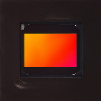
MT9V022I77ATC Aptina LLC, MT9V022I77ATC Datasheet - Page 8

MT9V022I77ATC
Manufacturer Part Number
MT9V022I77ATC
Description
IC SENSOR IMAGE VGA COLOR 52IBGA
Manufacturer
Aptina LLC
Type
CMOS Imagingr
Series
DigitalClarity®r
Specifications of MT9V022I77ATC
Pixel Size
6µm x 6µm
Active Pixel Array
752H x 480V
Frames Per Second
60
Voltage - Supply
3.3V
Package / Case
52-IBGA
Sensor Image Color Type
Color
Sensor Image Size Range
250,920 to 480,000Pixels
Sensor Image Size
752x480Pixels
Operating Supply Voltage (min)
3V
Operating Supply Voltage (typ)
3.3V
Operating Supply Voltage (max)
3.6V
Operating Temp Range
-40C to 85C
Package Type
IBGA
Operating Temperature Classification
Industrial
Mounting
Surface Mount
Pin Count
52
Lead Free Status / RoHS Status
Lead free / RoHS Compliant
Other names
557-1267
MT9V022I77ATC
MT9V022I77ATC
Ball Descriptions
Table 3:
PDF: 3295348826/Source:7478516499
MT9V022_DS - Rev.H 6/10 EN
52-Ball IBGA
Numbers
H7
D2
D1
C2
C1
H3
H4
H6
G7
H8
G8
A5
G4
G3
G5
H2
G2
G1
H1
H5
G6
B7
A8
A7
B6
A6
B5
B3
B2
A3
F8
E1
F1
F2
Ball Descriptions
Only pins D
BYPASS_CLKIN_N
SER_DATAOUT_N
SHFT_CLKOUT_N
BYPASS_CLKIN_P
SHFT_CLKOUT_P
SER_DATAIN_N
SER_DATAIN_P
FRAME_VALID
OUT
S_CTRL_ADR0
S_CTRL_ADR1
STFRM_OUT
LINE_VALID
STLN_OUT
EXPOSURE
STANDBY
LED_OUT
Symbol
RESET#
SYSCLK
0 through D
PIXCLK
ERROR
D
D
D
D
D
D
D
D
D
D
S
RSVD
SCLK
DATA
OUT
OUT
OUT
OUT
OUT
OUT
OUT
OUT
OUT
OUT
OE
5
6
7
8
9
4
3
2
1
0
OUT
9 may be tri-stated.
Output
Output
Output
Output
Output
Output
Output
Output
Output
Output
Output
Output
Output
Output
Output
Output
Output
Output
Input
Input
Input
Input
Input
Input
Input
Input
Input
Input
Input
Input
Input
Type
I/O
I/O
I/O
Connect to D
Serial data in for stereoscopy (differential negative). Tie to
1KΩ pull-up (to 3.3V) in non-stereoscopy mode.
Serial data in for stereoscopy (differential positive). Tie to
D
Input bypass shift-CLK (differential negative). Tie to 1KΩ pull-
up (to 3.3V) in non-stereoscopy mode.
Input bypass shift-CLK (differential positive). Tie to D
non-stereoscopy mode.
Rising edge starts exposure in slave mode.
Two-wire serial interface clock. Connect to V
resistor even when no other two-wire serial interface
peripheral is attached.
D
Two-wire serial interface slave address bit 3.
Two-wire serial interface slave address bit 5.
Asynchronous reset. All registers assume defaults.
Shut down sensor operation for power saving.
Master clock (26.6 MHz).
Two-wire serial interface data. Connect to V
resistor even when no other two-wire serial interface
peripheral is attached.
Output in master mode
in-phase; input in slave mode.
Output in master mode
chip in-phase; input in slave mode.
Asserted when D
Asserted when D
Parallel pixel data output 5.
Parallel pixel data output 6.
Parallel pixel data output 7.
Parallel pixel data output 8
Parallel pixel data output 9.
Error detected. Directly connected to STEREO ERROR FLAG.
LED strobe output.
Parallel pixel data output 4.
Parallel pixel data output 3.
Parallel pixel data output 2.
Parallel pixel data output 1.
Parallel pixel data output 0.
Pixel clock out. D
Output shift CLK (differential negative).
Output shift CLK (differential positive).
Serial data out (differential negative).
8
GND
OUT
MT9V022: 1/3-Inch Wide-VGA Digital Image Sensor
enable pad, active HIGH.
in non-stereoscopy mode.
GND
.
OUT
OUT
OUT
is valid on rising edge of this clock.
data is valid.
data is valid.
—
—
Description
start line sync to drive slave chip
start frame sync to drive a slave
Aptina reserves the right to change products or specifications without notice.
©2005 Aptina Imaging Corporation. All rights reserved.
DD
DD
with 1.5K
with 1.5K
Ball Descriptions
GND
in
Note
1
2


