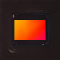
MT9V022I77ATC Aptina LLC, MT9V022I77ATC Datasheet - Page 23

MT9V022I77ATC
Manufacturer Part Number
MT9V022I77ATC
Description
IC SENSOR IMAGE VGA COLOR 52IBGA
Manufacturer
Aptina LLC
Type
CMOS Imagingr
Series
DigitalClarity®r
Specifications of MT9V022I77ATC
Pixel Size
6µm x 6µm
Active Pixel Array
752H x 480V
Frames Per Second
60
Voltage - Supply
3.3V
Package / Case
52-IBGA
Sensor Image Color Type
Color
Sensor Image Size Range
250,920 to 480,000Pixels
Sensor Image Size
752x480Pixels
Operating Supply Voltage (min)
3V
Operating Supply Voltage (typ)
3.3V
Operating Supply Voltage (max)
3.6V
Operating Temp Range
-40C to 85C
Package Type
IBGA
Operating Temperature Classification
Industrial
Mounting
Surface Mount
Pin Count
52
Lead Free Status / RoHS Status
Lead free / RoHS Compliant
Other names
557-1267
MT9V022I77ATC
MT9V022I77ATC
Signal Path
Figure 19:
On-Chip Biases
ADC Voltage Reference
V_Step Voltage Reference
Chip Version
PDF: 3295348826/Source:7478516499
MT9V022_DS - Rev.H 6/10 EN
Signal Path
The MT9V022 signal path consists of a programmable gain, a programmable analog
offset, and a 10-bit ADC. See “Black Level Calibration” on page 30 for the programmable
offset operation description.
The ADC voltage reference is programmed through R0x2C, bits 2:0. The ADC reference
ranges from 1.0V to 2.1V. The default value is 1.4V. The increment size of the voltage
reference is 0.1V from 1.0V to 1.6V (R0x2C[2:0] values 0 to 6). At R0x2C[2:0] = 7, the refer-
ence voltage jumps to 2.1V.
The effect of the ADC calibration does not scale with V
tive to the output of the analog gain stage. At default, one LSB of calibration equals two
LSB in output data (1LSB
It is very important to preserve the correct values of the other bits in R0x2C. The default
register setting is 0x0004.
This voltage is used for pixel high dynamic range operations, programmable from R0x31
through R0x34.
Chip version registers R0x00 and R0xFF are read-only.
Voltage (R0x48 or
Offset Correction
result of BLC)
(reset minus signal)
Pixel Output
S
Offset
23
C1
= 2mV, 1LSB
MT9V022: 1/3-Inch Wide-VGA Digital Image Sensor
C2
Gain Selection
result of AGC)
(R0x35 or
ADC
= 1mV).
Aptina reserves the right to change products or specifications without notice.
REF
. Instead it is a fixed value rela-
10 (12) bit ADC
©2005 Aptina Imaging Corporation. All rights reserved.
(R0x2C)
V
REF
Feature Description
ADC Data
(9:0)


