MT9M413C36STM Aptina LLC, MT9M413C36STM Datasheet - Page 10
MT9M413C36STM
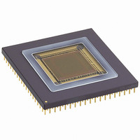
Manufacturer Part Number
MT9M413C36STM
Description
SENSOR IMAGE MONO CMOS 280-PGA
Manufacturer
Aptina LLC
Type
CMOS Imagingr
Specifications of MT9M413C36STM
Pixel Size
12µm x 12µm
Active Pixel Array
1280H x 1024V
Frames Per Second
500
Voltage - Supply
3.3V
Package / Case
280-PGA
Sensor Image Color Type
Monochrome
Sensor Image Size
1280x1024Pixels
Operating Supply Voltage (min)
3V
Operating Supply Voltage (max)
3.6V
Operating Temp Range
-5C to 60C
Package Type
CPGA
Operating Temperature Classification
Commercial
Mounting
Through Hole
Pin Count
280
Lead Free Status / RoHS Status
Contains lead / RoHS non-compliant
Other names
557-1153


Electronic Shutter
with the TrueSNAP freeze-frame electronic shutter, but
is also capable of operating in Electronic Rolling Shut-
ter (ERS) mode. With TrueSNAP the shutter can be
operated to generate continuous video output (simul-
taneous mode or sequential mode) or capture single
images (single frame mode).
modes it is useful to keep in mind the functionality of
PG_N and TX_N. When PG_N is low, the photodetector
is shorted to a reset voltage source. When high, the
switch is open. When TX_N is low, the photodetector is
shorted to pixel memory. When high, they are discon-
nected. Please refer to the switches shown in the Signal
Path Diagram, Figure 3 on page 3. The memory is also
reset during readout. It occurs for the selected row in
the middle of the 0-66 clock interval after application
of ROW_STRT_N (approximately clocks 20 through
40).
TrueSNAP Simultaneous Mode
being captured, the PG_N and TX_N signals are exer-
cised while the previous frame is being read out of the
sensor. In simultaneous mode typically the “end of
integration” occurs in the last row of the frame (row
#1023) or in the last row of the window of interest. The
position of the “start integration” is then calculated
from the desired integration time. Please note that
pixel memory is cleared during readout process
(Figure 9).
09005aef806807ca
MT9M413C36STC.fm - Ver. 3.0 1/04 EN
The MI-MV13 is intended to be operated primarily
When considering timing for the various shutter
In simultaneous mode, as a series of frames are
1.3-MEGAPIXEL CMOS ACTIVE-PIXEL
10
TrueSNAP Sequential Mode
exercised to control the integration time, and then dig-
itization and readout of the frame takes place. Please
note that pixel memory is cleared during readout pro-
cess. The photodetector is reset when PG_N is low.
Raising PG_N starts integration and lowering TX_N
while PG_N is still high ends integration by sampling
the signal into memory. There must be at least one
SYSCLK cycle after returning TX_N to the high state
until PG_N is lowered (Figure 10 on page 11).
Figure 9: Typical Example of TrueSNAP
ROW_ADDR
Simultaneous Mode: Exposure During
In sequential mode the PG_N and TX_N signals are
Micron Technology, Inc., reserves the right to change products or specifications without notice.
PG_N
TX_N
1023
0
n
DIGITAL IMAGE SENSOR
Readout
Readout
Exposure
time
©2004 Micron Technology, Inc. All rights reserved.
Readout
Time
Related parts for MT9M413C36STM
Image
Part Number
Description
Manufacturer
Datasheet
Request
R

Part Number:
Description:
SENSOR IMAGE VGA COLOR CMOS PLCC
Manufacturer:
Aptina LLC
Datasheet:

Part Number:
Description:
IC SENSOR IMAGE COLOR 48CLCC
Manufacturer:
Aptina LLC
Datasheet:

Part Number:
Description:
SENSOR IMAGE 1.3MP CMOS 48-CLCC
Manufacturer:
Aptina LLC
Datasheet:

Part Number:
Description:
SENSOR IMAGE 2MP CMOS 48-CLCC
Manufacturer:
Aptina LLC
Datasheet:

Part Number:
Description:
SENSOR IMAGE VGA MONO 52IBGA
Manufacturer:
Aptina LLC
Datasheet:

Part Number:
Description:
SENSOR IMAGE VGA COLOR 48CLCC
Manufacturer:
Aptina LLC
Datasheet:

Part Number:
Description:
SENSOR IMAGE COLOR CMOS 48-PLCC
Manufacturer:
Aptina LLC
Datasheet:

Part Number:
Description:
KIT HEAD BOARD FOR MT9P031
Manufacturer:
Aptina LLC
Datasheet:

Part Number:
Description:
KIT HEAD BOARD FOR MT9D131
Manufacturer:
Aptina LLC
Datasheet:

Part Number:
Description:
KIT HEAD BOARD FOR MT9P031
Manufacturer:
Aptina LLC
Datasheet:
Part Number:
Description:
SENSOR IMAGE VGA COLOR CMOS PLCC
Manufacturer:
Aptina LLC
Datasheet:
Part Number:
Description:
IC SENSOR IMAGE COLOR 48CLCC
Manufacturer:
Aptina LLC
Datasheet:
Part Number:
Description:
SENSOR IMAGE 2MP CMOS 48-CLCC
Manufacturer:
Aptina LLC
Datasheet:
