MT9M413C36STM Aptina LLC, MT9M413C36STM Datasheet - Page 6
MT9M413C36STM
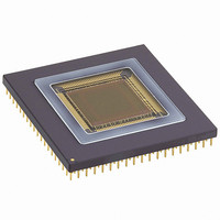
Manufacturer Part Number
MT9M413C36STM
Description
SENSOR IMAGE MONO CMOS 280-PGA
Manufacturer
Aptina LLC
Type
CMOS Imagingr
Specifications of MT9M413C36STM
Pixel Size
12µm x 12µm
Active Pixel Array
1280H x 1024V
Frames Per Second
500
Voltage - Supply
3.3V
Package / Case
280-PGA
Sensor Image Color Type
Monochrome
Sensor Image Size
1280x1024Pixels
Operating Supply Voltage (min)
3V
Operating Supply Voltage (max)
3.6V
Operating Temp Range
-5C to 60C
Package Type
CPGA
Operating Temperature Classification
Commercial
Mounting
Through Hole
Pin Count
280
Lead Free Status / RoHS Status
Contains lead / RoHS non-compliant
Other names
557-1153


PG_N and TX_N
resets the photodetectors for the entire pixel array. To
end integration, the TX_N signal simultaneously trans-
fers charge from photodetector to memory inside each
pixel for the entire pixel array. In sequential mode the
PG_N and the TX_N pulses must have a minimum
duration of 64 SYSCLK cycles. In simultaneous mode
the PG_N and TX_N pulses must have a duration of 64
SYSCLK cycles and be applied in the window between
the 66th and 129th SYSCLK cycles. Additionally, in
simultaneous mode between exposures a single
SYSCLK duration pulse must be applied each row dur-
ing the 130th clock cycle.
ROW_ADDR
externally via this 10-bit input bus. Must be valid for at
least 66 SYSCLK cycles, must be valid when
ROW_STRT_N is pulled low.
09005aef806807ca
MT9M413C36STC.fm - Ver. 3.0 1/04 EN
To start integration, the PG_N signal simultaneously
The address for the pixel row to be read is input
Controller
Controller
ROW_ADDR
ROW_ADDR
ROW_STRT_N
ROW_STRT_N
LD_SHFT_N
SYSCLK
SYSCLK
Figure 5: Example 1 - Row 4 of the MI-MV13 Being Digitized
0
0
0
0
0
0
0
0
0
0
0
0
0
0
1
1
0
0
0
0
1. Reads the contents of pixel row specified by ROW_ADDR
1. Reads the contents of pixel row specified by ROW_ADDR
2. Converts pixel row signals to digital values
2. Converts pixel row signals to digital values
3. Stores digital values in ADC register (1280 x 10 bit)
3. Stores digital values in ADC register (1280 x 10 bit)
Decoders
Decoders
Control
Control
Logic/
Logic/
Control s
Control s
Control s
Control s
ADC
ADC
ADC
ADC
1.3-MEGAPIXEL CMOS ACTIVE-PIXEL
6
ROW_STRT_N
fied by ROW_ADDR, converts the pixel row signal to
digital value, and stores the digital value in ADC regis-
ter (1280 x 10-bit).
cycles. Must be valid for a minimum of two clock
cycles and a maximum of 100 clock cycles.
ROW_DONE_N
been pulled low the sensor acknowledges the comple-
tion of a row read operation/digitization by sending
out a low going pulse on this pin. Valid for two clock
cycles.
Column Parallel 10 -bit
Column Parallel 10 -bit
This signal reads the contents of the pixel row speci-
This process is completed in 128-129
128-129
Column Parallel 10 -bit
Column Parallel 10 -bit
1. In order to minimize the sensor power con-
Micron Technology, Inc., reserves the right to change products or specifications without notice.
ADC 640 x 1
ADC 640 x 1
PIXEL ARRAY
PIXEL ARRAY
sumption, the row processing circuitry
operates at SYSCLK/2. Therefore, depend-
ing on the user’s implementation, there will
be either 128 or 129 SYSCLK cycles between
the start of ROW_STRT_N and
ROW_DONE_N.
ADC 640 x 1
ADC 640 x 1
ROW 4
ROW 4
1
SYSCLK cycles after ROW_STRT_N has
DIGITAL IMAGE SENSOR
©2004 Micron Technology, Inc. All rights reserved.
Even
Even
Columns
Columns
Odd
Odd
Columns
Columns
1
SYSCLK
Related parts for MT9M413C36STM
Image
Part Number
Description
Manufacturer
Datasheet
Request
R

Part Number:
Description:
SENSOR IMAGE VGA COLOR CMOS PLCC
Manufacturer:
Aptina LLC
Datasheet:

Part Number:
Description:
IC SENSOR IMAGE COLOR 48CLCC
Manufacturer:
Aptina LLC
Datasheet:

Part Number:
Description:
SENSOR IMAGE 1.3MP CMOS 48-CLCC
Manufacturer:
Aptina LLC
Datasheet:

Part Number:
Description:
SENSOR IMAGE 2MP CMOS 48-CLCC
Manufacturer:
Aptina LLC
Datasheet:

Part Number:
Description:
SENSOR IMAGE VGA MONO 52IBGA
Manufacturer:
Aptina LLC
Datasheet:

Part Number:
Description:
SENSOR IMAGE VGA COLOR 48CLCC
Manufacturer:
Aptina LLC
Datasheet:

Part Number:
Description:
SENSOR IMAGE COLOR CMOS 48-PLCC
Manufacturer:
Aptina LLC
Datasheet:

Part Number:
Description:
KIT HEAD BOARD FOR MT9P031
Manufacturer:
Aptina LLC
Datasheet:

Part Number:
Description:
KIT HEAD BOARD FOR MT9D131
Manufacturer:
Aptina LLC
Datasheet:

Part Number:
Description:
KIT HEAD BOARD FOR MT9P031
Manufacturer:
Aptina LLC
Datasheet:
Part Number:
Description:
SENSOR IMAGE VGA COLOR CMOS PLCC
Manufacturer:
Aptina LLC
Datasheet:
Part Number:
Description:
IC SENSOR IMAGE COLOR 48CLCC
Manufacturer:
Aptina LLC
Datasheet:
Part Number:
Description:
SENSOR IMAGE 2MP CMOS 48-CLCC
Manufacturer:
Aptina LLC
Datasheet:
