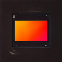
MT9V022IA7ATM Aptina LLC, MT9V022IA7ATM Datasheet - Page 51

MT9V022IA7ATM
Manufacturer Part Number
MT9V022IA7ATM
Description
SENSOR IMAGE VGA MONO 52IBGA
Manufacturer
Aptina LLC
Type
CMOS Imagingr
Series
DigitalClarity®r
Specifications of MT9V022IA7ATM
Pixel Size
6µm x 6µm
Active Pixel Array
752H x 480V
Frames Per Second
60
Voltage - Supply
3.3V
Package / Case
52-IBGA
Sensor Image Color Type
Monochrome
Sensor Image Size Range
250,920 to 480,000Pixels
Sensor Image Size
752x480Pixels
Operating Supply Voltage (min)
3V
Operating Supply Voltage (typ)
3.3V
Operating Supply Voltage (max)
3.6V
Operating Temp Range
-40C to 85C
Package Type
IBGA
Operating Temperature Classification
Industrial
Mounting
Surface Mount
Pin Count
52
Lead Free Status / RoHS Status
Lead free / RoHS Compliant
Other names
557-1205
Available stocks
Company
Part Number
Manufacturer
Quantity
Price
Broadcast and Individual Writes for Stereoscopic Topology
Figure 48:
PDF: 3295348826/Source:7478516499
MT9V022_DS - Rev.H 6/10 EN
Two-Wire Serial Interface Configuration in Stereoscopic Mode
In stereoscopic mode, the two sensors are required to run in lockstep. This implies that
control logic in each sensor is in exactly the same state as its pair on every clock. To
ensure this, all inputs that affect control logic must be identical and arrive at the same
time at each sensor.
These inputs include:
• system clock
• system reset
• two-wire serial interface clk - SCL
• two-wire serial interface data - SDA
The setup in Figure 48 shows how the two sensors can maintain lockstep when their
configuration registers are written through the two-wire serial interface. A WRITE to
configuration registers would either be broadcast (simultaneous WRITES to both
sensors) or individual (WRITE to just one sensor at a time). READs from configuration
registers would be individual (READs from just one sensor at a time).
One of the two serial interface slave address bits of the sensor is hardwired. The other is
controlled by the host. This allows the host to perform either a broadcast or a one-to-
one access.
Broadcast WRITES are performed by setting the same S_CTRL_ADR input bit for both
slave and master sensor. Individual WRITES are performed by setting opposite
S_CTRL_ADR input bit for both slave and master sensor. Similarly, individual READs are
performed by setting opposite S_CTRL_ADR input bit for both slave and master sensor.
26.6 MHz
Osc.
All system clock lengths (L) must be equal.
SCL and SDA lengths to each sensor (from the host) must also be equal.
HOST
L
CLK
SCL
SDA
L
S_CTRL_ADR[0]
SCL
51
SENSOR
SLAVE
Host launches SCL and SDA on positive
edge of SYSCLK.
MT9V022: 1/3-Inch Wide-VGA Digital Image Sensor
L
SDA
CLK
S_CTRL_ADR[0]
Appendix A – Serial Configurations
SCL
Aptina reserves the right to change products or specifications without notice.
MASTER
SENSOR
©2005 Aptina Imaging Corporation. All rights reserved.
SDA
CLK


