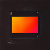
MT9V022IA7ATM Aptina LLC, MT9V022IA7ATM Datasheet - Page 26

MT9V022IA7ATM
Manufacturer Part Number
MT9V022IA7ATM
Description
SENSOR IMAGE VGA MONO 52IBGA
Manufacturer
Aptina LLC
Type
CMOS Imagingr
Series
DigitalClarity®r
Specifications of MT9V022IA7ATM
Pixel Size
6µm x 6µm
Active Pixel Array
752H x 480V
Frames Per Second
60
Voltage - Supply
3.3V
Package / Case
52-IBGA
Sensor Image Color Type
Monochrome
Sensor Image Size Range
250,920 to 480,000Pixels
Sensor Image Size
752x480Pixels
Operating Supply Voltage (min)
3V
Operating Supply Voltage (typ)
3.3V
Operating Supply Voltage (max)
3.6V
Operating Temp Range
-40C to 85C
Package Type
IBGA
Operating Temperature Classification
Industrial
Mounting
Surface Mount
Pin Count
52
Lead Free Status / RoHS Status
Lead free / RoHS Compliant
Other names
557-1205
Available stocks
Company
Part Number
Manufacturer
Quantity
Price
Exposure Indicator
High Dynamic Range
Figure 21:
Figure 22:
PDF: 3295348826/Source:7478516499
MT9V022_DS - Rev.H 6/10 EN
Sequence of Control Voltages at the HDR Gate
Sequence of Voltages in a Piecewise Linear Pixel Response
The exposure indicator is controlled by:
• R0x1B LED_OUT Control
The MT9V022 provides an output pin, LED_OUT, to indicate when the exposure takes
place. When R0x1B bit 0 is clear, LED_OUT is HIGH during exposure. By using R0x1B, bit
1, the polarity of the LED_OUT pin can be inverted.
High dynamic range is controlled by:
• R0x08 Shutter Width 1
• R0x09 Shutter Width 2
• R0x0A Shutter Width Control
• R0x31
In the MT9V022, high dynamic range (that is, R0x0F, bit 6 = 1) is achieved by controlling
the saturation level of the pixel (HDR or high dynamic range gate) during the exposure
period. The sequence of the control voltages at the HDR gate is shown in Figure 21. After
the pixels are reset, the step voltage, V_Step, which is applied to HDR gate, is setup at V1
for integration time t
V4, which also serves as an antiblooming voltage for the photodetector. This sequence of
voltages leads to a piecewise linear pixel response, illustrated (in approximates) in
Figure 21 on page 26.
Voltage
HDR
1/t
–
1
R0x34 V_Step Voltages
V
AA
dV1
1/t
1
(3.3V)
then to V2 for time t
2
t
1
26
V1~1.4V
MT9V022: 1/3-Inch Wide-VGA Digital Image Sensor
dV2
Light Intensity
1/t
3
2
Exposure
, then V3 for time t
V2~1.2V
Aptina reserves the right to change products or specifications without notice.
t
dV3
2
3
, and finally it is parked at
©2005 Aptina Imaging Corporation. All rights reserved.
V3~1.0V
t
3
Feature Description
V4~0.8V


