AD8349ARE Analog Devices Inc, AD8349ARE Datasheet - Page 6
AD8349ARE
Manufacturer Part Number
AD8349ARE
Description
IC QUADRATURE MOD 700MHZ 16TSSOP
Manufacturer
Analog Devices Inc
Datasheet
1.AD8349AREZ-RL7.pdf
(28 pages)
Specifications of AD8349ARE
Rohs Status
RoHS non-compliant
Function
Modulator
Lo Frequency
700MHz ~ 2.7GHz
Rf Frequency
700MHz ~ 2.7GHz
P1db
5.6dBm
Noise Floor
-156dBm/Hz
Output Power
5.1dBm
Current - Supply
150mA
Voltage - Supply
4.75 V ~ 5.5 V
Test Frequency
2.14GHz
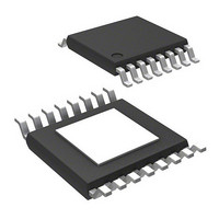
Package / Case
16-TSSOP (0.173", 4.40mm Width) Exposed pad
Available stocks
Company
Part Number
Manufacturer
Quantity
Price

Part Number:
AD8349ARE
Manufacturer:
ADI/亚德诺
Quantity:
20 000
Part Number:
AD8349AREZ
Manufacturer:
ADI/亚德诺
Quantity:
20 000
Part Number:
AD8349AREZ-REEL7
Manufacturer:
ADI/亚德诺
Quantity:
20 000
Part Number:
AD8349AREZ-RL7
Manufacturer:
ADI/亚德诺
Quantity:
20 000


AD8349
PIN CONFIGURATION AND FUNCTIONAL DESCRIPTIONS
Table 3. Pin Function Descriptions
Pin No.
1, 2,
15, 16
3, 4
5, 6
7
8
9
10, 13,
14
11
12
Mnemonic
IBBP, IBBN,
QBBN, QBBP
COM1
LOIN, LOIP
VPS1
ENOP
COM2
COM3
VOUT
VPS2
Description
Differential In-Phase and Quadrature Baseband Inputs. These high impedance inputs must be
dc-biased to approximately 400 mV dc, and must be driven from a low impedance source.
Nominal characterized ac signal swing is 600 mV p-p on each pin (100 mV to 700 mV). This
results in a differential drive of 1.2 V p-p with a 400 mV dc bias. These inputs are not self-biased
and must be externally biased.
Common Pin for LO Phase Splitter and LO Buffers. COM1, COM2, and COM3 should all be
connected to a ground plane via a low impedance path.
Differential Local Oscillator Inputs. Internally dc-biased to approximately 1.8 V when V
Pins must be ac-coupled. Single-ended drive is possible with degradation in performance.
Positive Supply Voltage (4.75 V to 5.5 V) for the LO Bias-Cell and Buffer. VPS1 and VPS2 should
be connected to the same supply. To ensure adequate external bypassing, connect 0.1 µF and
100 pF capacitors between VPS1 and ground.
Output Enable. This pin can be used to enable or disable the RF output. Connect to high logic
level for normal operation. Connect to low logic level to disable output.
Common Pin for the Output Amplifier. COM1, COM2, and COM3 should all be connected to a
ground plane via a low impedance path.
Common Pin for Input V-to-I Converters and Mixer Cores. COM1, COM2, and COM3 should all
be connected to a ground plane via a low impedance path.
Device Output. Single-ended, 50 Ω internally biased RF output. Pin must be ac-coupled to the
load.
Positive Supply Voltage (4.75 V to 5.5 V) for the Baseband Input V-to-I Converters, Mixer Core,
Band Gap Reference, and Output Amplifer. VPS1 and VPS2 should be connected to the same
supply. To ensure adequate external bypassing, connect 0.1 µF and 100 pF capacitors between
VPS2 and ground.
COM1
COM1
ENOP
VPS1
IBBN
IBBP
LOIN
LOIP
1
2
3
4
5
6
7
8
Rev. A | Page 6 of 28
(Not to Scale)
AD8349
TOP VIEW
Figure 2.
16
15
14
13
12
11
10
9
QBBP
QBBN
COM3
COM3
VPS2
VOUT
COM3
COM2
S
= 5.0 V.
Equivalent
Circuit
Circuit A
Circuit B
Circuit C
Circuit D
Related parts for AD8349ARE
Image
Part Number
Description
Manufacturer
Datasheet
Request
R

Part Number:
Description:
±1.7g Dual-Axis IMEMS Accelerometer Evaluation Board
Manufacturer:
Analog Devices Inc
Datasheet:

Part Number:
Description:
Inertial Sensor Evaluation System
Manufacturer:
Analog Devices Inc
Datasheet:
Part Number:
Description:
Manufacturer:
Analog Devices Inc
Datasheet:
Part Number:
Description:
Manufacturer:
Analog Devices Inc
Datasheet:
Part Number:
Description:
Manufacturer:
Analog Devices Inc
Datasheet:
Part Number:
Description:
Manufacturer:
Analog Devices Inc
Datasheet:
Part Number:
Description:
Manufacturer:
Analog Devices Inc
Datasheet:
Part Number:
Description:
Manufacturer:
Analog Devices Inc
Datasheet:
Part Number:
Description:
Manufacturer:
Analog Devices Inc
Datasheet:
Part Number:
Description:
Manufacturer:
Analog Devices Inc
Datasheet:
Part Number:
Description:
Manufacturer:
Analog Devices Inc
Datasheet:
Part Number:
Description:
Manufacturer:
Analog Devices Inc
Datasheet:
Part Number:
Description:
Manufacturer:
Analog Devices Inc
Datasheet: