AD8349ARE Analog Devices Inc, AD8349ARE Datasheet - Page 3
AD8349ARE
Manufacturer Part Number
AD8349ARE
Description
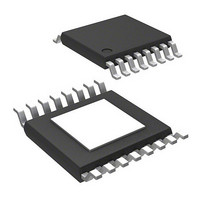
IC QUADRATURE MOD 700MHZ 16TSSOP
Manufacturer
Analog Devices Inc
Datasheet
1.AD8349AREZ-RL7.pdf
(28 pages)
Specifications of AD8349ARE
Rohs Status
RoHS non-compliant
Function
Modulator
Lo Frequency
700MHz ~ 2.7GHz
Rf Frequency
700MHz ~ 2.7GHz
P1db
5.6dBm
Noise Floor
-156dBm/Hz
Output Power
5.1dBm
Current - Supply
150mA
Voltage - Supply
4.75 V ~ 5.5 V
Test Frequency
2.14GHz
Package / Case
16-TSSOP (0.173", 4.40mm Width) Exposed pad
Available stocks
Company
Part Number
Manufacturer
Quantity
Price

Part Number:
AD8349ARE
Manufacturer:
ADI/亚德诺
Quantity:
20 000
Part Number:
AD8349AREZ
Manufacturer:
ADI/亚德诺
Quantity:
20 000
Part Number:
AD8349AREZ-REEL7
Manufacturer:
ADI/亚德诺
Quantity:
20 000
Part Number:
AD8349AREZ-RL7
Manufacturer:
ADI/亚德诺
Quantity:
20 000


SPECIFICATIONS
V
bias; baseband frequency = 1 MHz; LO source and RF output load impedances are 50 Ω, unless otherwise noted.
Table 1.
Parameter
Operating Frequency
LO = 900 MHz
LO = 1900 MHz
LO = 2140 MHz
LO INPUTS
BASEBAND INPUTS
S
Output Power
Output P1 dB
Carrier Feedthrough
Sideband Suppression
Third Harmonic
Output IP3
Quadrature Error
I/Q Amplitude Balance
Noise Floor
GSM Sideband Noise
Output Power
Output P1dB
Carrier Feedthrough
Sideband Suppression
Third Harmonic
Output IP3
Quadrature Error
I/Q Amplitude Balance
Noise Floor
GSM Sideband Noise
Output Power
Output P1dB
Carrier Feedthrough
Sideband Suppression
Third Harmonic
Output IP3
Quadrature Error
I/Q Amplitude Balance
Noise Floor
WCDMA Noise Floor
LO Drive Level
Nominal Impedance
Input Return Loss
I and Q Input Bias Level
Input Bias Current
Input Offset Current
Bandwidth (0.1 dB)
= 5 V; ambient temperature (T
1
1
1
Conditions
P
F1
20 MHz offset from LO, all BB inputs 400 mV dc bias only
20 MHz offset from LO, BB inputs = 1.2 V p-p differential on 400 mV dc
LO = 884.8 MHz, 6 MHz offset from LO, P
P
F1
20 MHz offset from LO, all BB inputs 400 mV dc bias only
20 MHz offset from LO, BB inputs = 1.2 V p-p differential on 400 mV dc
LO = 1960 MHz, 6 MHz offset from LO, P
P
F1
20 MHz offset from LO, all BB inputs 400 mV dc bias only
20 MHz offset from LO, BB inputs = 1.2 V p-p differential on 400 mV dc
LO = 2140 MHz. 30 MHz offset from LO, P
Pins LOIP and LOIN
Characterization performed at typical level
Drive via 1:1 balun, LO = 2140 MHz
Pins IBBP, IBBN, QBBP, QBBN
LO = 1500 MHz, baseband input = 600 mV p-p sine wave on 400 mV dc
LO = 1500 MHz, baseband input = 60 mV p-p sine wave on 400 mV dc
A
OUT
OUT
OUT
) = 25°C; LO = –6 dBm; I/Q inputs = 1.2 V p-p differential sine waves in quadrature on a 400 mV dc
BB
BB
BB
– (F
– (F
– (F
= 3 MHz, F2
= 3 MHz, F2
= 3 MHz, F2
LO
LO
LO
+ (3 × F
+ (3 × F
+ (3 × F
BB
BB
BB
BB
BB
BB
= 4 MHz, P
= 4 MHz, P
= 4 MHz, P
)), P
)), P
)), P
OUT
OUT
OUT
= 4 dBm
= 3.8 dBm
= 2.4 dBm
Rev. A | Page 3 of 28
OUT
OUT
OUT
= -4.2 dBm
= –4.5 dBm
= –6.5 dBm
OUT
OUT
CHAN
= 2 dBm
= 2 dBm
= –17.3 dBm
Min
700
1.5
0
–2
–10
Typ
4
7.6
–45
–35
–39
21
1.9
0.1
–155
–150
–152
3.8
6.8
–38
–40
–37
22
0.7
0.1
–156
–150
–151
2.4
5.6
–42
–43
–37
19
0.3
0.1
–156
–151
–156
–6
50
–8.6
400
11
1.8
10
24
–30
–36
–30
–36
Max
2700
6
–31
–36
6
–36
5.1
–36
0
AD8349
Unit
MHz
dBm
dBm
dBm
dBc
dBc
dBm
degree
dB
dBm/Hz
dBm/Hz
dBc/Hz
dBm
dBm
dBm
dBc
dBc
dBm
degree
dB
dBm/Hz
dBm/Hz
dBc/Hz
dBm
dBm
dBm
dBc
dBc
dBm
degree
dB
dBm/Hz
dBm/Hz
dBm/Hz
dBm
Ω
dB
mV
µA
µA
MHz
MHz
Related parts for AD8349ARE
Image
Part Number
Description
Manufacturer
Datasheet
Request
R

Part Number:
Description:
±1.7g Dual-Axis IMEMS Accelerometer Evaluation Board
Manufacturer:
Analog Devices Inc
Datasheet:

Part Number:
Description:
Inertial Sensor Evaluation System
Manufacturer:
Analog Devices Inc
Datasheet:
Part Number:
Description:
Manufacturer:
Analog Devices Inc
Datasheet:
Part Number:
Description:
Manufacturer:
Analog Devices Inc
Datasheet:
Part Number:
Description:
Manufacturer:
Analog Devices Inc
Datasheet:
Part Number:
Description:
Manufacturer:
Analog Devices Inc
Datasheet:
Part Number:
Description:
Manufacturer:
Analog Devices Inc
Datasheet:
Part Number:
Description:
Manufacturer:
Analog Devices Inc
Datasheet:
Part Number:
Description:
Manufacturer:
Analog Devices Inc
Datasheet:
Part Number:
Description:
Manufacturer:
Analog Devices Inc
Datasheet:
Part Number:
Description:
Manufacturer:
Analog Devices Inc
Datasheet:
Part Number:
Description:
Manufacturer:
Analog Devices Inc
Datasheet:
Part Number:
Description:
Manufacturer:
Analog Devices Inc
Datasheet: