AD8349ARE Analog Devices Inc, AD8349ARE Datasheet - Page 15

AD8349ARE
Manufacturer Part Number
AD8349ARE
Description
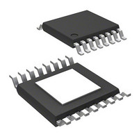
IC QUADRATURE MOD 700MHZ 16TSSOP
Manufacturer
Analog Devices Inc
Datasheet
1.AD8349AREZ-RL7.pdf
(28 pages)
Specifications of AD8349ARE
Rohs Status
RoHS non-compliant
Function
Modulator
Lo Frequency
700MHz ~ 2.7GHz
Rf Frequency
700MHz ~ 2.7GHz
P1db
5.6dBm
Noise Floor
-156dBm/Hz
Output Power
5.1dBm
Current - Supply
150mA
Voltage - Supply
4.75 V ~ 5.5 V
Test Frequency
2.14GHz
Package / Case
16-TSSOP (0.173", 4.40mm Width) Exposed pad
Available stocks
Company
Part Number
Manufacturer
Quantity
Price
Part Number:
AD8349ARE
Manufacturer:
ADI/亚德诺
Quantity:
20 000
Part Number:
AD8349AREZ
Manufacturer:
ADI/亚德诺
Quantity:
20 000
Part Number:
AD8349AREZ-REEL7
Manufacturer:
ADI/亚德诺
Quantity:
20 000
Part Number:
AD8349AREZ-RL7
Manufacturer:
ADI/亚德诺
Quantity:
20 000
BASIC CONNECTIONS
The basic connections for operating the AD8349 are shown in
Figure 43. A single power supply of between 4.75 V and 5.5 V is
applied to pins VPS1 and VPS2. A pair of ESD protection diodes
connect internally between VPS1 and VPS2, so these must be
tied to the same potential. Both pins should be individually
decoupled using 100 pF and 0.1 μF capacitors to ground. These
capacitors should be located as close as possible to the device.
For normal operation, the output enable pin, ENOP, must be
pulled high. The turn-on threshold for ENOP is 2 V. Pins
COM1, COM2, and COM3 should all be tied to the same
ground plane through low impedance paths.
BASEBAND I AND Q INPUTS
The I and Q inputs should be driven differentially. The typical
differential drive level (as used for characterization measure-
ments) for the I and Q baseband signals is 1.2 V p-p, which is
equivalent to 600 mV p-p on each baseband input. The base-
band inputs have to be externally biased to a level between
400 mV and 500 mV. The optimum level for the best perfor-
mance is 400 mV. The recommended drive level of 1.2 V p-p
does not indicate a maximum drive level. If operation closer to
compression is desired, the 1.2 V p-p differential limit can be
exceeded.
For baseband signals with a high peak-to-average ratio (e.g.,
CDDA or WCDMA), the peak signal level will have to be below
the AD8349’s compression level in order to prevent clipping of
the signal peaks. Clipping of signal peaks increases distortion.
In the case of CDMA and WCDMA inputs, clipping results in
an increase of signal leakage into adjacent channels. In general,
the baseband drive should be at a level where the peak signal
+V
LO
IN
IP
S
5
4
0.1µF
ETC1-1-13
T1
200Ω
200Ω
1
2
3
100pF
100pF
100pF
Figure 43. Basic Connections
1
2
3
4
5
6
7
8
Rev. A | Page 15 of 28
IBBP
IBBN
COM1
COM1
LOIN
LOIP
VPS1
ENOP
AD8349
power of the output signal is at least a crest factor below the
AD8349’s output compression point. Refer to the Applications
section for drive-level considerations in WCDMA and
GSM/EDGE systems.
Reducing the baseband drive level also has the benefit of
increasing the bandwidth of the baseband input. This would
allow the AD8349 to be used in applications requiring a high
modulation bandwidth, e.g., as the IF modulator in high data-
rate microwave radios.
SINGLE-ENDED BASEBAND DRIVE
Where only single-ended I and Q signals are available, a
differential amplifier, such as the AD8132 or AD8138, can be
used to generate the required differential drive signal for the
AD8349.
Figure 44 shows an example of a circuit that converts a ground-
referenced, single-ended signal to a differential signal, and adds
the required 400 mV bias voltage.
The baseband inputs can also be driven with a single-ended
signal biased to 400 mV, with the unused inputs biased to
400 mV dc. This mode of operation is not recommended,
however, because any dc level difference between the bias level
of the drive signal and the dc level on the unused input
(including the effect of temperature drift), can result in
increased LO feedthrough. Additionally, the maximum low
distortion output power will be reduced by 6 dB.
QBBN
QBBP
COM3
COM3
COM3
COM2
VOUT
VPS2
16
15
14
13
12
11
10
9
100pF
100pF
0.1µF
QP
QN
+V
VOUT
S
AD8349


