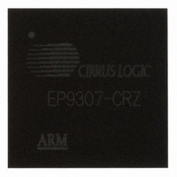
EP9307-CRZR Cirrus Logic Inc, EP9307-CRZR Datasheet - Page 38

EP9307-CRZR
Manufacturer Part Number
EP9307-CRZR
Description
IC Universal Platform ARM9 SOC Prcessor
Manufacturer
Cirrus Logic Inc
Series
EP9r
Specifications of EP9307-CRZR
Core Processor
ARM9
Core Size
16/32-Bit
Speed
200MHz
Connectivity
EBI/EMI, Ethernet, I²C, IrDA, Keypad/Touchscreen, SPI, UART/USART, USB
Peripherals
AC'97, DMA, I²:S, LCD, LED, MaverickKey, POR, PWM, WDT
Number Of I /o
14
Program Memory Type
ROMless
Ram Size
32K x 8
Voltage - Supply (vcc/vdd)
1.65 V ~ 3.6 V
Data Converters
A/D 8x12b
Oscillator Type
External
Operating Temperature
0°C ~ 70°C
Package / Case
272-LFBGA
Processor Series
EP93xx
Core
ARM920T
Data Bus Width
32 bit
3rd Party Development Tools
MDK-ARM, RL-ARM, ULINK2
Development Tools By Supplier
EDB9307A-Z
Lead Free Status / RoHS Status
Lead free / RoHS Compliant
Eeprom Size
-
Program Memory Size
-
Lead Free Status / Rohs Status
Details
Other names
Q5809834A
Available stocks
Company
Part Number
Manufacturer
Quantity
Price
Company:
Part Number:
EP9307-CRZR
Manufacturer:
Cirrus Logic Inc
Quantity:
10 000
EP9307
ARM9 SOC with Ethernet, USB, Display and Touchscreen
ADC
Using the ADC:
This ADC has a state-machine based conversion engine that automates the conversion process. The initiator for a
conversion is the read access of the TSXYResult register by the CPU. The data returned from reading this register
contains the result as well as the status bit indicating the state of the ADC. However, this peripheral requires a delay
between each successful conversion and the issue of the next conversion command, or else the returned value of
successive samples may not reflect the analog input. Since the state of the ADC state machine is returned through the
same channel used to initiate the conversion process, there must be a delay inserted after every complete conversion.
Note that reading TSXYResult during a conversion will not affect the result of the ongoing process.
The following is a recommended procedure for safely polling the ADC from software:
38
Resolution
Integral non-linearity
Offset error
Full scale error
Maximum sample rate
Channel switch settling time
Noise (RMS) - typical
Note:
1. Read the TSXYResult register into a local variable to initiate a conversion.
2. If the value of bit 31 of the local variable is '0' then repeat step 1.
3. Delay long enough to meet the maximum sample rate as shown above.
4. Mask the local variable with 0xFFFF to remove extraneous data.
5. If signed mode is used, do a sign extend of the lower halfword.
6. Return the sampled value.
ADIV refers to bit 16 in the KeyTchClkDiv register.
ADIV = 0 means the input clock to the ADC module is equal to the external 14.7456 MHz clock divided by 4.
ADIV = 1 means the input clock to the ADC module is equal to the external 14.7456 MHz clock divided by 16.
Parameter
Copyright 2010 Cirrus Logic (All Rights Reserved)
FFFF
61A8
9E58
0000
0
Figure 24. ADC Transfer Function
Range of 0 to 3.3 V
A/D Converter Transfer Function
No missing codes
(approximately ±25,000 counts)
Comment
ADIV = 0
ADIV = 1
ADIV = 0
ADIV = 1
Vref/2
50K counts (approximate)
Vref
Value
0.01%
0.2%
3750
±15
925
500
120
2
Samples per second
Samples per second
Units
mV
ms
μV
μs
DS667F2


