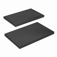
CY7C1474V25-200BGXI Cypress Semiconductor Corp, CY7C1474V25-200BGXI Datasheet - Page 16

CY7C1474V25-200BGXI
Manufacturer Part Number
CY7C1474V25-200BGXI
Description
CY7C1474V25-200BGXI
Manufacturer
Cypress Semiconductor Corp
Datasheet
1.CY7C1470V25-200BZXC.pdf
(31 pages)
Specifications of CY7C1474V25-200BGXI
Format - Memory
RAM
Memory Type
SRAM - Synchronous
Memory Size
72M (1M x 72)
Speed
200MHz
Interface
Parallel
Voltage - Supply
2.375 V ~ 2.625 V
Operating Temperature
-40°C ~ 85°C
Package / Case
209-FBGA
Density
72Mb
Access Time (max)
3ns
Sync/async
Synchronous
Architecture
SDR
Clock Freq (max)
200MHz
Operating Supply Voltage (typ)
2.5V
Address Bus
20b
Package Type
FBGA
Operating Temp Range
-40C to 85C
Number Of Ports
8
Supply Current
450mA
Operating Supply Voltage (min)
2.375V
Operating Supply Voltage (max)
2.625V
Operating Temperature Classification
Industrial
Mounting
Surface Mount
Pin Count
209
Word Size
72b
Number Of Words
1M
Lead Free Status / RoHS Status
Lead free / RoHS Compliant
Lead Free Status / RoHS Status
Lead free / RoHS Compliant
Available stocks
Company
Part Number
Manufacturer
Quantity
Price
Company:
Part Number:
CY7C1474V25-200BGXI
Manufacturer:
Cypress Semiconductor Corp
Quantity:
135
Company:
Part Number:
CY7C1474V25-200BGXI
Manufacturer:
Cypress Semiconductor Corp
Quantity:
10 000
Part Number:
CY7C1474V25-200BGXI
Manufacturer:
CYPRESS/赛普拉斯
Quantity:
20 000
Scan Register Sizes
Identification Codes
Document Number: 38-05290 Rev. *L
Instruction
Bypass
ID
Boundary scan order–165-ball FBGA
Boundary scan order–209-ball BGA
EXTEST
IDCODE
SAMPLE Z
RESERVED
SAMPLE/PRELOAD
RESERVED
RESERVED
BYPASS
Instruction
Register Name
Code
000
001
010
100
101
011
110
111
Captures I/O ring contents. Places the boundary scan register between TDI and TDO. Forces
all SRAM outputs to high Z state. This instruction is not 1149.1-compliant.
Loads the ID register with the vendor ID code and places the register between TDI and TDO.
This operation does not affect SRAM operations.
Captures I/O ring contents. Places the boundary scan register between TDI and TDO. Forces
all SRAM output drivers to a high Z state.
Do Not Use: This instruction is reserved for future use.
Captures I/O ring contents. Places the boundary scan register between TDI and TDO. Does not
affect SRAM operation. This instruction does not implement 1149.1 preload function and is
therefore not 1149.1-compliant.
Do Not Use: This instruction is reserved for future use.
Do Not Use: This instruction is reserved for future use.
Places the bypass register between TDI and TDO. This operation does not affect SRAM
operations.
Bit Size (× 36)
32
71
3
1
–
Description
Bit Size (× 18)
32
52
3
1
–
Bit Size (× 72)
CY7C1470V25
CY7C1472V25
CY7C1474V25
110
32
3
1
–
Page 16 of 31
[+] Feedback


