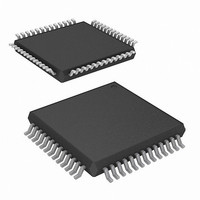
CY7B9945V-2AXC Cypress Semiconductor Corp, CY7B9945V-2AXC Datasheet - Page 4

CY7B9945V-2AXC
Manufacturer Part Number
CY7B9945V-2AXC
Description
CY7B9945V-2AXC
Manufacturer
Cypress Semiconductor Corp
Series
RoboClock™r
Type
Clock Buffer, Fanout Distributionr
Datasheets
1.CY7B9945V-2AXC.pdf
(15 pages)
2.CY7B9945V-2AXC.pdf
(10 pages)
3.CY7B9945V-2AXC.pdf
(13 pages)
Specifications of CY7B9945V-2AXC
Pll
Yes
Input
LVPECL, LVTTL
Output
LVTTL
Number Of Circuits
1
Ratio - Input:output
4:10
Differential - Input:output
Yes/No
Frequency - Max
200MHz
Divider/multiplier
Yes/Yes
Voltage - Supply
2.97 V ~ 3.63 V
Operating Temperature
0°C ~ 70°C
Mounting Type
Surface Mount
Package / Case
52-LQFP
Frequency-max
200MHz
Number Of Elements
1
Supply Current
250mA
Pll Input Freq (min)
24MHz
Pll Input Freq (max)
200MHz
Operating Supply Voltage (typ)
3.3V
Operating Temp Range
0C to 70C
Package Type
TQFP
Output Frequency Range
24 to 200MHz
Operating Supply Voltage (min)
2.97V
Operating Supply Voltage (max)
3.63V
Operating Temperature Classification
Commercial
Pin Count
52
Lead Free Status / RoHS Status
Lead free / RoHS Compliant
Lead Free Status / RoHS Status
Lead free / RoHS Compliant
Other names
428-2909
CY7B9945V-2AXC
CY7B9945V-2AXC
Available stocks
Company
Part Number
Manufacturer
Quantity
Price
Company:
Part Number:
CY7B9945V-2AXC
Manufacturer:
CYPRESS
Quantity:
672
Company:
Part Number:
CY7B9945V-2AXC
Manufacturer:
Cypress Semiconductor Corp
Quantity:
10 000
Company:
Part Number:
CY7B9945V-2AXCT
Manufacturer:
Cypress Semiconductor Corp
Quantity:
10 000
Document #: 38-07336 Rev. *E
Output Disable Description
The output of each output bank can be independently put into
a HOLD-OFF or high-impedance state. The combination of the
MODE and DIS[1:2] inputs determines the clock outputs’ state
for each bank. When the DIS[1:2] is LOW, the outputs of the
corresponding banks will be enabled. When DIS[1:2] is HIGH,
the outputs for that bank will be disabled to a high-impedance
(HI-Z) or HOLD-OFF state. Table 5 defines the disabled
outputs functions.
The HOLD-OFF state is intended to be a power saving feature.
An output bank is disabled to the HOLD-OFF state in a
maximum of six output clock cycles from the time when the
disable input is HIGH. When disabled to the HOLD-OFF state,
Note:
(N/A)
(N/A)
(N/A)
3.
1F[1:0]
1F[3:2]
(N/A)
(N/A)
(N/A)
MM
LM
LH
ML
MH
LL
HL
HM
HH
FB connected to an output selected for “Zero” skew (i.e., FBF0 = MID or XF[1:0] = MID).
(N/A)
(N/A)
(N/A)
(N/A)
(N/A)
(N/A)
(N/A)
(N/A)
2F[1:0]
MM
HL
LL
LM
HM
LH
HH
REFInput
FBInput
+1t
+2t
+3t
+6t
+7t
+8t
–2t
+4t
–8t
–7t
–6t
–4t
–3t
–1t
0t
Figure 1. Typical Outputs with FB Connected to a Zero-Skew Output
U
U
U
U
U
U
U
U
U
U
U
U
U
U
U
outputs are driven to a logic LOW state on their falling edges.
This ensures the output clocks are stopped without a glitch.
When a bank of outputs is disabled to HI-Z state, the
respective bank of outputs will go HI-Z immediately.
Table 5. DIS[1:2] Functionality
HIGH/LOW
MODE
HIGH
LOW
MID
DIS[1:2]
HIGH
HIGH
LOW
X
[3]
RoboClock
1Q[0:3], 2Q[0:5]
FACTORY TEST
CY7B9945V
HOLD-OFF
ENABLED
HI-Z
Page 4 of 10
[+] Feedback


