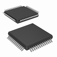
CY7B9945V-2AXC Cypress Semiconductor Corp, CY7B9945V-2AXC Datasheet - Page 2

CY7B9945V-2AXC
Manufacturer Part Number
CY7B9945V-2AXC
Description
CY7B9945V-2AXC
Manufacturer
Cypress Semiconductor Corp
Series
RoboClock™r
Type
Clock Buffer, Fanout Distributionr
Datasheets
1.CY7B9945V-2AXC.pdf
(15 pages)
2.CY7B9945V-2AXC.pdf
(10 pages)
3.CY7B9945V-2AXC.pdf
(13 pages)
Specifications of CY7B9945V-2AXC
Pll
Yes
Input
LVPECL, LVTTL
Output
LVTTL
Number Of Circuits
1
Ratio - Input:output
4:10
Differential - Input:output
Yes/No
Frequency - Max
200MHz
Divider/multiplier
Yes/Yes
Voltage - Supply
2.97 V ~ 3.63 V
Operating Temperature
0°C ~ 70°C
Mounting Type
Surface Mount
Package / Case
52-LQFP
Frequency-max
200MHz
Number Of Elements
1
Supply Current
250mA
Pll Input Freq (min)
24MHz
Pll Input Freq (max)
200MHz
Operating Supply Voltage (typ)
3.3V
Operating Temp Range
0C to 70C
Package Type
TQFP
Output Frequency Range
24 to 200MHz
Operating Supply Voltage (min)
2.97V
Operating Supply Voltage (max)
3.63V
Operating Temperature Classification
Commercial
Pin Count
52
Lead Free Status / RoHS Status
Lead free / RoHS Compliant
Lead Free Status / RoHS Status
Lead free / RoHS Compliant
Other names
428-2909
CY7B9945V-2AXC
CY7B9945V-2AXC
Available stocks
Company
Part Number
Manufacturer
Quantity
Price
Company:
Part Number:
CY7B9945V-2AXC
Manufacturer:
CYPRESS
Quantity:
672
Company:
Part Number:
CY7B9945V-2AXC
Manufacturer:
Cypress Semiconductor Corp
Quantity:
10 000
Company:
Part Number:
CY7B9945V-2AXCT
Manufacturer:
Cypress Semiconductor Corp
Quantity:
10 000
Document #: 38-07336 Rev. *E
Pin Definitions
34
40,39,
36,37
38
42
28,18,
35,17,
2, 1
19,26
14,12,
13,3
29
50,51
48,46,
32,30,
5,7,8,10
, 20,22
44
52
25
6,9,21,
31, 45,
47
16,27,
41
4,11,15,
23,24,
33,43,4
9
Pin
FS
REFA+, REFA-
REFB+, REFB-
REFSEL
FBK
1F[0:3], 2F[0:1]
DIS[1:2]
[1:2]DS[0:1]
FBF0
FBDS[0:1]
1Q[0:3], 2Q[0:5]
QF
LOCK
MODE
VCCN
VCCQ
GND
Name
Output
Output
Output
Input
Input
Input
Input
Input
Input
Input
Input
Input
Input
I/O
3-level Input Output Phase Function Select. Each pair determines the phase of the
3-level Input Output Divider Function Select. Each pair determines the divider ratio of
3-level Input Feedback Output Phase Function Select. This input determines the phase
3-level Input Feedback Output Divider Function Select. This input determines the
3-level Input This pin determines the clock outputs’ disable state. When this input is
Three-level
LVDIFF
LVTTL/
LVTTL
LVTTL
LVTTL
LVTTL
LVTTL
LVTTL
Type
PWR
PWR
PWR
Input
Frequency Select. This input must be set according to the nominal frequency
(f
Reference Inputs. These inputs can operate as differential PECL or
single-ended TTL reference inputs to the PLL. When operating as a
single-ended LVTTL input, the complementary input must be left open.
Reference Select Input. The REFSEL input controls how the reference input
is configured. When LOW, it will use the REFA pair as the reference input.
When HIGH, it will use the REFB pair as the reference input. This input has
an internal pull-down.
Feedback Input Clock. The PLL will operate such that the rising edges of
the reference and feedback signals are aligned in phase and frequency. This
pin is used to feedback the clock output QF to the phase detector.
respective bank of outputs. See Table 3.
Output Disable. Each input controls the state of the respective output bank.
When HIGH, the output bank is disabled to “HOLD-OFF” or “High-Z” state;
the disable state is determined by MODE. When LOW, outputs 1Q[0:3] and
2Q[0:5] are enabled. See Table 5.
the respective bank of outputs. See Table 4.
of the QF output. See Table 3.
divider ratio of the QF output. See Table 4.
Clock Outputs with Adjustable Phases and f
output frequencies and phases are determined by [1:2]DS[0:1], and 1F[0:3]
and 2F[0:1], respectively. See Table 3 and Table 4.
Feedback Clock Output. This output is intended to be connected to the FBK
input. The output frequency and phase are determined by FBDS[0:1] and
FBF0, respectively. See Table 3 and 4.
PLL Lock Indicator. When HIGH, this output indicates the internal PLL is
locked to the reference signal. When LOW, it indicates that the PLL is
attempting to acquire lock
HIGH, the clock outputs will disable to high impedance state (High-Z). When
this input is LOW, the clock outputs will disable to HOLD-OFF mode. When
in MID, the device will enter factory test mode.
Power Supply for the Output Buffers
Power Supply for the Internal Circuitry
Device Ground
NOM
). See Table 1.
Description
NOM
Divide Ratios. The
RoboClock
CY7B9945V
Page 2 of 10
[+] Feedback


