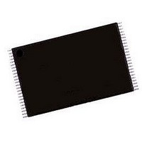
AM29LV641DH120REF Spansion Inc., AM29LV641DH120REF Datasheet - Page 4

AM29LV641DH120REF
Manufacturer Part Number
AM29LV641DH120REF
Description
Flash Memory IC
Manufacturer
Spansion Inc.
Datasheet
1.AM29LV641DH90REI.pdf
(57 pages)
Specifications of AM29LV641DH120REF
Memory Size
64Mbit
Memory Configuration
4M X 16
Ic Interface Type
Parallel
Access Time
120ns
Memory Case Style
TSOP
No. Of Pins
48
Operating Temperature Range
-40°C To +85°C
Termination Type
SMD
Lead Free Status / RoHS Status
Lead free / RoHS Compliant
GENERAL DESCRIPTION
The Am29LV640DU/Am29LV641DU is a 64 Mbit, 3.0
Volt (3.0 V to 3.6 V) single power supply flash memory
device organized as 4,194,304 words. Data appears
on DQ0-DQ15. The device is designed to be pro-
grammed in-system with the standard system 3.0 volt
V
or erase operations. You can also program this device
in standard EPROM programmers.
Access times of 90 and 120 ns are available for appli-
cations where V
available for applications where V
is offered in 48-pin TSOP, 56-pin SSOP, 63-ball
Fine-Pitch BGA and 64-ball Fortified BGA packages.
To eliminate bus contention, each device has separate
chip enable (CE#), write enable (WE#), and output en-
able (OE#) controls.
Each device requires only a single 3.0 Volt power
supply (3.0 V to 3.6 V) for both read and write func-
tions. Internally generated and regulated voltages are
provided for the program and erase operations.
The device is entirely command set compatible with
the JEDEC single-power-supply Flash standard.
Commands are written to the command register using
standard microprocessor write timing. Register con-
tents serve as inputs to an internal state-machine that
controls the erase and programming circuitry. Write
cycles also internally latch addresses and data
needed for the programming and erase operations.
Reading data out of the device is similar to reading
from other Flash or EPROM devices.
Device programming occurs by executing the program
command sequence. This initiates the Embedded
Program algorithm — an internal algorithm that auto-
matically times the program pulse widths and verifies
proper cell margin. The Unlock Bypass mode facili-
tates faster programming times by requiring only two
write cycles to program data instead of four.
Device erasure occurs by executing the erase com-
mand sequence. This initiates the Embedded Erase
algorithm — an internal algorithm that automatically
preprograms the array (if it is not already programmed)
before executing the erase operation. During erase,
the device automatically times the erase pulse widths
and verifies proper cell margin.
The VersatileIO™ (V
to set the voltage levels that the device generates and
tolerates on CE# and DQ I/Os to the same voltage
level that is asserted on V
configurations (1.8–2.9 V and 3.0–5.0 V) for operation
in various system environments.
The host system can detect whether a program or
erase operation is complete by observing the RY/BY#
pin, by reading the DQ7 (Data# Polling), or DQ6 (tog-
2
CC
supply. A 12.0 volt V
IO
≥ V
IO
CC
) control allows the host system
PP
. An access time 120 ns are
is not required for program
IO
. V
IO
IO
is available in two
< V
CC
. The device
Am29LV640D/Am29LV641D
D A T A
S H E E T
gle) status bits. After a program or erase cycle com-
pletes, the device is ready to read array data or accept
another command.
The sector erase architecture allows memory sec-
tors to be erased and reprogrammed without affecting
the data contents of other sectors. The device is fully
erased when shipped from the factory.
Hardware data protection measures include a low
V
tions during power transitions. The hardware sector
protection feature disables both program and erase
operations in any combination of sectors of memory.
This is achieved in-system or via programming equip-
ment.
The Erase Suspend/Erase Resume feature enables
the user to put erase on hold for any period of time to
read data from, or program data to, any sector that is
not selected for erasure. True background erase can
thus be achieved.
The hardware RESET# pin terminates any operation
in progress and resets the internal state machine to
reading array data. The RESET# pin can be tied to the
system reset circuitry. A system reset would thus also
reset the device, enabling the system microprocessor
to read boot-up firmware from the Flash memory de-
vice.
The device offers a standby mode as a power-saving
feature. Once the system places the device into the
standby mode, power consumption is greatly reduced.
The SecSi (Secured Silicon) Sector provides an
minimum 128-word area for code or data that can be
permanently protected. Once this sector is protected,
no further programming or erasing within the sector
can occur.
The Write Protect (WP#) feature protects the first or
last sector by asserting a logic low on the WP# pin.
The protected sector is still protected even during ac-
celerated programming.
The accelerated program (ACC) feature allows the
system to program the device at a much faster rate.
When ACC is pulled high to V
Unlock Bypass mode, enabling the user to reduce the
time needed to do the program operation. This feature
is intended to increase factory throughput during sys-
tem production, but may also be used in the field if de-
sired.
AMD’s Flash technology combines years of Flash
memory manufacturing experience to produce the
highest levels of quality, reliability and cost effective-
ness. The device electrically erases all bits within a
sector simultaneously via Fowler-Nordheim tunnelling.
The data is programmed using hot electron injection.
CC
detector that automatically inhibits write opera-
HH
22366C6 January 22, 2007
, the device enters the


