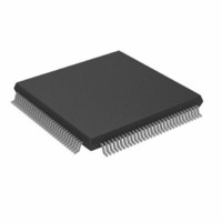
ADV611JSTZ Analog Devices Inc, ADV611JSTZ Datasheet - Page 34

ADV611JSTZ
Manufacturer Part Number
ADV611JSTZ
Description
CCTV Digital Video Codec
Manufacturer
Analog Devices Inc
Type
Video Codecr
Datasheet
1.ADV611JSTZ.pdf
(46 pages)
Specifications of ADV611JSTZ
Data Interface
Serial
Resolution (bits)
8 b
Sigma Delta
No
Voltage - Supply, Digital
4.5 V ~ 5.5 V
Operating Temperature
0°C ~ 70°C
Mounting Type
Surface Mount
Package / Case
120-LQFP
Lead Free Status / RoHS Status
Lead free / RoHS Compliant
Available stocks
Company
Part Number
Manufacturer
Quantity
Price
Company:
Part Number:
ADV611JSTZ
Manufacturer:
ADI
Quantity:
526
Company:
Part Number:
ADV611JSTZ
Manufacturer:
Analog Devices Inc
Quantity:
10 000
Part Number:
ADV611JSTZ
Manufacturer:
ADI
Quantity:
20 000
ADV611/ADV612
TEST CONDITIONS
Figure 22 shows test condition voltage reference and device
loading information. These test conditions consider an output
as disabled when the output stops driving and goes from the
measured high or low voltage to a high impedance state. Tests
measure output disable time (t
reference input signal crossing +1.5 V and the time that the
TIMING PARAMETERS
This section contains signal timing information for the ADV611/ADV612. Timing descriptions for the following items appear in this
section:
• Clock signal timing
• Video data transfer timing (CCIR-656, and Multiplexed Philips formats)
• Host data transfer timing (direct register read/write access)
Clock Signal Timing
The diagram in this section shows timing for VCLK input and VCLKO output. All output values assume a maximum pin
loading of 50 pF.
Video Format
CCIR-601 PAL
CCIR-601 NTSC
NOTES
1
2
VCLK Duty Cycle
NOTE
1
Parameter
t
t
t
VCLK Period Drift = 0.1 (VCLK_CYC/field.
VCLK edge-to-edge jitter = 1 ns.
VCLK Duty Cycle = t
VCLK_CYC
VCLKO_D0
VCLKO_D1
REFERENCE
OUTPUT
SIGNAL
SIGNAL
INPUT
Description
VCLK Signal, Cycle Time (1/Frequency) at 27 MHz
VCLKO Signal, Delay (when VCLK2 = 0) at 27 MHz
VCLKO Signal, Delay (when VCLK2 = 1) at 27 MHz
V
V
V
VCLK_HI
V
1
IH
IL
OH
OL
INPUT & OUTPUT VOLTAGE/TIMING REFERENCES
/(t
VCLK_LO
DISABLE
Figure 22. Test Condition Voltage Reference and Device Loading
)
100.
Min VCLK_CYC
Period
35.2 ns
35.2 ns
Table XVII. Video Clock Period, Frequency, Drift and Jitter
1.5V
) as the time between the
t
DISABLED
Table XIX. Video Clock Timing Parameters
Table XVIII. Video Clock Duty Cycle
Min
(40%)
1.5V
–34–
Nominal VCLK_CYC
Period (Frequency)
37 ns (27 MHz)
37 ns (27 MHz)
output reaches the high impedance state (also +1.5 V). Simi-
larly, these tests conditions consider an output as enabled when
the output leaves the high impedance state and begins driving a
measured high or low voltage. Tests measure output enable time
(t
+1.5 V and the time that the output reaches the measured high
or low voltage.
ENABLE
t
ENABLED
) as the time between the reference input signal crossing
DEVICE LOADING FOR AC MEASUREMENTS
Nominal
(50%)
Min
(See Video Clock Period Table)
10
10
OUTPUT
PIN
TO
2pF
I
I
Max VCLK_CYC
Period
38.9 ns
38.9 ns
Max
29
29
OH
OL
1, 2
+1.5V
Max
(60%)
Unit
ns
ns
REV. 0


