ADSP-21262SBBC-150 Analog Devices Inc, ADSP-21262SBBC-150 Datasheet - Page 35
ADSP-21262SBBC-150
Manufacturer Part Number
ADSP-21262SBBC-150
Description
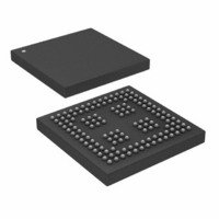
IC,DSP,32-BIT,CMOS,BGA,136PIN,PLASTIC
Manufacturer
Analog Devices Inc
Series
SHARC®r
Type
Fixed/Floating Pointr
Specifications of ADSP-21262SBBC-150
Interface
DAI, SPI
Clock Rate
150MHz
Non-volatile Memory
ROM (512 kB)
On-chip Ram
256kB
Voltage - I/o
3.30V
Voltage - Core
1.20V
Operating Temperature
-40°C ~ 85°C
Mounting Type
Surface Mount
Package / Case
136-CSPBGA
Device Core Size
32/40Bit
Architecture
Super Harvard
Format
Floating Point
Clock Freq (max)
150MHz
Mips
150
Device Input Clock Speed
150MHz
Ram Size
256KB
Program Memory Size
512KB
Operating Supply Voltage (typ)
1.2/3.3V
Operating Supply Voltage (min)
1.14/3.13V
Operating Supply Voltage (max)
1.26/3.47V
Operating Temp Range
0C to 70C
Operating Temperature Classification
Commercial
Mounting
Surface Mount
Pin Count
136
Package Type
CSPBGA
Lead Free Status / RoHS Status
Contains lead / RoHS non-compliant
Lead Free Status / RoHS Status
Contains lead / RoHS non-compliant
Available stocks
Company
Part Number
Manufacturer
Quantity
Price
Company:

Part Number:
ADSP-21262SBBC-150
Manufacturer:
Analog Devices Inc
Quantity:
10 000


SPI Protocol—Slave
See
Table 30. SPI Protocol—Slave
Parameter
Timing Requirements
t
t
t
t
t
t
t
t
Switching Characteristics
t
t
t
t
t
SPICLKS
SPICHS
SPICLS
SDSCO
HDS
SSPIDS
HSPIDS
SDPPW
DSOE
DSDHI
DDSPIDS
HDSPIDS
DSOV
Table 30
and
Figure
Serial Clock Cycle
Serial Clock High Period
Serial Clock Low Period
SPIDS Assertion to First SPICLK Edge
CPHASE = 0
CPHASE = 1
Last SPICLK Edge to SPIDS Not Asserted CPHASE = 0
Data Input Valid to SPICLK Edge (Data Input Setup Time)
SPICLK Last Sampling Edge to Data Input Not Valid
SPIDS Deassertion Pulse Width (CPHASE = 0)
SPIDS Assertion to Data Out Active
SPIDS Deassertion to Data High Impedance
SPICLK Edge to Data Out Valid (Data Out Delay Time)
SPICLK Edge to Data Out Not Valid (Data Out Hold Time)
SPIDS Assertion to Data Out Valid (CPHASE = 0)
26.
Rev. B | Page 35 of 48 | August 2005
2 × t
Min
4 × t
2 × t
2 × t
2 × t
2 × t
2 × t
2
2
2 × t
0
0
CCLK
CCLK
CCLK
CCLK
CCLK
CCLK
CCLK
CCLK
– 2
– 2
+ 1
+ 1
– 2
Max
5
5
7.5
5 × t
CCLK
+ 2
ADSP-21262
Unit
ns
ns
ns
ns
ns
ns
ns
ns
ns
ns
ns
ns
ns
ns
Related parts for ADSP-21262SBBC-150
Image
Part Number
Description
Manufacturer
Datasheet
Request
R

Part Number:
Description:
±1.7g Dual-Axis IMEMS Accelerometer Evaluation Board
Manufacturer:
Analog Devices Inc
Datasheet:

Part Number:
Description:
Inertial Sensor Evaluation System
Manufacturer:
Analog Devices Inc
Datasheet:
Part Number:
Description:
Manufacturer:
Analog Devices Inc
Datasheet:
Part Number:
Description:
Manufacturer:
Analog Devices Inc
Datasheet:
Part Number:
Description:
Manufacturer:
Analog Devices Inc
Datasheet:
Part Number:
Description:
Manufacturer:
Analog Devices Inc
Datasheet:
Part Number:
Description:
Manufacturer:
Analog Devices Inc
Datasheet:
Part Number:
Description:
Manufacturer:
Analog Devices Inc
Datasheet:
Part Number:
Description:
Manufacturer:
Analog Devices Inc
Datasheet:
Part Number:
Description:
Manufacturer:
Analog Devices Inc
Datasheet:
Part Number:
Description:
Manufacturer:
Analog Devices Inc
Datasheet:
Part Number:
Description:
Manufacturer:
Analog Devices Inc
Datasheet:
Part Number:
Description:
Manufacturer:
Analog Devices Inc
Datasheet: