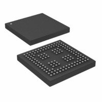
ADSP-21262SBBC-150 Analog Devices Inc, ADSP-21262SBBC-150 Datasheet - Page 27

ADSP-21262SBBC-150
Manufacturer Part Number
ADSP-21262SBBC-150
Description
IC,DSP,32-BIT,CMOS,BGA,136PIN,PLASTIC
Manufacturer
Analog Devices Inc
Series
SHARC®r
Type
Fixed/Floating Pointr
Specifications of ADSP-21262SBBC-150
Interface
DAI, SPI
Clock Rate
150MHz
Non-volatile Memory
ROM (512 kB)
On-chip Ram
256kB
Voltage - I/o
3.30V
Voltage - Core
1.20V
Operating Temperature
-40°C ~ 85°C
Mounting Type
Surface Mount
Package / Case
136-CSPBGA
Device Core Size
32/40Bit
Architecture
Super Harvard
Format
Floating Point
Clock Freq (max)
150MHz
Mips
150
Device Input Clock Speed
150MHz
Ram Size
256KB
Program Memory Size
512KB
Operating Supply Voltage (typ)
1.2/3.3V
Operating Supply Voltage (min)
1.14/3.13V
Operating Supply Voltage (max)
1.26/3.47V
Operating Temp Range
0C to 70C
Operating Temperature Classification
Commercial
Mounting
Surface Mount
Pin Count
136
Package Type
CSPBGA
Lead Free Status / RoHS Status
Contains lead / RoHS non-compliant
Lead Free Status / RoHS Status
Contains lead / RoHS non-compliant
Available stocks
Company
Part Number
Manufacturer
Quantity
Price
Company:
Part Number:
ADSP-21262SBBC-150
Manufacturer:
Analog Devices Inc
Quantity:
10 000
Memory Write—Parallel Port
Use the specifications in
Figure 20
memory-mapped peripherals) when the ADSP-21262 is access-
ing external memory space.
Table 21. 8-Bit Memory Write Cycle
1
Parameter
Switching Characteristics
t
t
t
t
t
t
t
t
t
t
t
D = (data cycle duration) × t
H = t
On reset, ALE is an active high cycle. However, it can be reconfigured by software to be active low.
ALEW
ALERW
ADAS
ADAH
WW
ADWL
ADWH
ALEHZ
DWS
DWH
DAWH
CCLK
(if a hold cycle is specified, else H = 0)
for asynchronous interfacing to memories (and
AD15-8
AD7-0
ALE
ALE Pulse Width
ALE Deasserted to Read/Write Asserted
Address/Data15–0 Setup Before ALE Deasserted
Address/Data15–0 Hold After ALE Deasserted
WR Pulse Width
Address/Data15–8 to WR Low
Address/Data15–8 Hold After WR High
ALE Deasserted
Address/Data7–0 Setup Before WR High
Address/Data7–0 Hold After WR High
Address/Data to WR High
WR
RD
Table
CCLK
21,
Table
1
to Address/Data15–0 in High Z
VALID ADDRESS
VALID ADDRESS
22,
t
ADAS
t
ALEW
Figure
Rev. B | Page 27 of 48 | August 2005
19, and
Figure 19. 8-Bit Memory Write Cycle
t
ADAH
t
ALEHZ
t
ALERW
1
1
t
ADWL
VALID ADDRESS
t
DAW H
Min
2 × t
1 × t
2.5 × t
0.5 × t
D – 2
0.5 × t
0.5 × t
0.5 × t
D
0.5 × t
D
t
WW
CCLK
CCLK
VALID DATA
CCLK
CCLK
CCLK
CCLK
CCLK
CCLK
t
DWS
– 2
– 0.5
– 2.0
– 0.8
– 1.5
– 1 + H
– 0.8
– 1.5 + H
t
DWH
t
ADWH
Max
0.5t
CCLK
ADSP-21262
+ 2.0
Unit
ns
ns
ns
ns
ns
ns
ns
ns
ns
ns
ns


