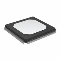
ADSP-21061KSZ-133 Analog Devices Inc, ADSP-21061KSZ-133 Datasheet - Page 12

ADSP-21061KSZ-133
Manufacturer Part Number
ADSP-21061KSZ-133
Description
ADSP-21061 1MBIT, 33MHz, 5v SHARC
Manufacturer
Analog Devices Inc
Series
SHARC®r
Type
Floating Pointr
Datasheet
1.ADSP-21061LKSZ-160.pdf
(56 pages)
Specifications of ADSP-21061KSZ-133
Interface
Synchronous Serial Port (SSP)
Clock Rate
33MHz
Non-volatile Memory
External
On-chip Ram
128kB
Voltage - I/o
5.00V
Voltage - Core
5.00V
Operating Temperature
0°C ~ 85°C
Mounting Type
Surface Mount
Package / Case
240-MQFP, 240-PQFP
Package
240MQFP
Numeric And Arithmetic Format
Floating-Point
Maximum Speed
33 MHz
Ram Size
128 KB
Device Million Instructions Per Second
33 MIPS
Lead Free Status / RoHS Status
Lead free / RoHS Compliant
Available stocks
Company
Part Number
Manufacturer
Quantity
Price
Company:
Part Number:
ADSP-21061KSZ-133
Manufacturer:
Analog Devices Inc
Quantity:
10 000
ADSP-21061/ADSP-21061L
Table 2. Pin Descriptions (Continued)
Pin
TFSx
RFSx
EBOOT
LBOOT
BMS
CLKIN
RESET
TCK
TMS
TDI
TDO
TRST
EMU
ICSA
VDD
GND
NC
A = Asynchronous, G = Ground, I = Input, O = Output, P = Power Supply, S = Synchronous, (A/D) = Active Drive, (O/D) = Open-Drain,
T = Three-State (when SBTS is asserted, or when the ADSP-21061 is a bus slave)
Type
I/O
I/O
I
I
I/O/T*
I
I/A
I
I/S
I/S
O
I/A
O
O
P
G
Function
Transmit Frame Sync (Serial Ports 0, 1).
Receive Frame Sync (Serial Ports 0, 1).
EPROM Boot Select. When EBOOT is high, the ADSP-21061 is configured for booting from an 8-bit EPROM.
When EBOOT is low, the LBOOT and BMS inputs determine booting mode. See the table in the BMS pin
description below. This signal is a system configuration selection that should be hardwired.
Link Boot. Must be tied to GND.
Boot Memory Select. Output: Used as chip select for boot EPROM devices (when EBOOT = 1,
LBOOT = 0). In a multiprocessor system, BMS is output by the bus master. Input: When low, indicates that no
booting will occur and that ADSP-21061 will begin executing instructions from external memory. See table
below. This input is a system configuration selection that should be hardwired. *Three-statable only in
EPROM boot mode (when BMS is an output).
EBOOT
1
0
0
Clock In. External clock input to the ADSP-21061. The instruction cycle rate is equal to CLKIN. CLKIN may
not be halted, changed, or operated below the minimum specified frequency.
Processor Reset. Resets the ADSP-21061 to a known state and begins program execution at the program
memory location specified by the hardware reset vector address. This input must be asserted (low) at
power-up.
Test Clock (JTAG). Provides an asynchronous clock for JTAG boundary scan.
Test Mode Select (JTAG). Used to control the test state machine. TMS has a 20 kΩ internal pull-up resistor.
Test Data Input (JTAG). Provides serial data for the boundary scan logic. TDI has a 20 kΩ internal pull-up
resistor.
Test Data Output (JTAG). Serial scan output of the boundary scan path.
Test Reset (JTAG). Resets the test state machine. TRST must be asserted (pulsed low) after power-up or held
low for proper operation of the ADSP-21061. TRST has a 20 kΩ internal pull-up resistor.
Emulation Status. Must be connected to the ADSP-21061 EZ-ICE target board connector only. EMU has a
50 kΩ internal pull-up resistor.
Reserved. Leave unconnected.
Power Supply. Nominally 5.0 V dc for 5 V devices or 3.3 V dc for 3.3 V devices. (30 pins)
Power Supply Return. (30 pins)
Do Not Connect. Reserved pins which must be left open and unconnected.
0
0
0
LBOOT
Rev. C | Page 12 of 56 | July 2007
BMS
Output
1(Input)
0 (Input)
Booting Mode
EPROM (Connect BMS to EPROM chip select.)
No Booting. Processor executes from external memory.
Host Processor.


