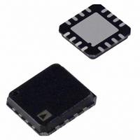
ADL5534ACPZ-R7 Analog Devices Inc, ADL5534ACPZ-R7 Datasheet - Page 6

ADL5534ACPZ-R7
Manufacturer Part Number
ADL5534ACPZ-R7
Description
Dual 5531
Manufacturer
Analog Devices Inc
Datasheet
1.ADL5534ACPZ-R7.pdf
(16 pages)
Specifications of ADL5534ACPZ-R7
Design Resources
Interfacing ADL5534 to AD9640 High Speed ADC (CN0049)
Current - Supply
98mA ~ 110mA
Frequency
20MHz ~ 500MHz
Gain
19dB ~ 20.5dB
Noise Figure
3dB
P1db
20.4dBm
Package / Case
16-VQFN, 16-CSP, Exposed Pad
Rf Type
General Purpose
Test Frequency
380MHz
Voltage - Supply
4.75 V ~ 5.25 V
Lead Free Status / RoHS Status
Lead free / RoHS Compliant
Other names
ADL5534ACPZ-R7TR
ADL5534
PIN CONFIGURATION AND FUNCTION DESCRIPTIONS
Table 4. Pin Function Descriptions
Pin No.
1, 2, 3, 4, 6, 9,
10, 11, 14, 15
5, 16
7, 12
8, 13
NC
RFIN2, RFIN1
RFOUT2, RFOUT1
Exposed Paddle
Mnemonic
CLIN2, CLIN1
Description
No Connect.
RF Input. Requires a dc blocking capacitor. Use a 10 nF capacitor for normal operation.
A 1 nF capacitor connected from Pin 7 to ground and Pin12 to ground provides decoupling
for the on-board linearizer.
RF Output and Bias. DC bias is provided to this pin through an inductor. A 470 nH inductor is
recommended for normal operation. The RF path requires a dc blocking capacitor. Use a 10 nF
capacitor for normal operation.
GND. Solder this paddle to a low impedance ground plane.
NC 1
NC 2
NC 3
NC 4
Figure 2. Pin Configuration
Rev. 0 | Page 6 of 16
(Not to Scale)
PIN 1
INDICATOR
ADL5534
TOP VIEW
12
11
10
9
CLIN1
NC
NC
NC


