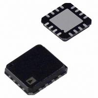
ADL5534ACPZ-R7 Analog Devices Inc, ADL5534ACPZ-R7 Datasheet - Page 12

ADL5534ACPZ-R7
Manufacturer Part Number
ADL5534ACPZ-R7
Description
Dual 5531
Manufacturer
Analog Devices Inc
Datasheet
1.ADL5534ACPZ-R7.pdf
(16 pages)
Specifications of ADL5534ACPZ-R7
Design Resources
Interfacing ADL5534 to AD9640 High Speed ADC (CN0049)
Current - Supply
98mA ~ 110mA
Frequency
20MHz ~ 500MHz
Gain
19dB ~ 20.5dB
Noise Figure
3dB
P1db
20.4dBm
Package / Case
16-VQFN, 16-CSP, Exposed Pad
Rf Type
General Purpose
Test Frequency
380MHz
Voltage - Supply
4.75 V ~ 5.25 V
Lead Free Status / RoHS Status
Lead free / RoHS Compliant
Other names
ADL5534ACPZ-R7TR
ADL5534
SOLDERING INFORMATION AND RECOMMENDED
PCB LAND PATTERN
Figure 22 shows the recommended land pattern for ADL5534.
To minimize thermal impedance, the exposed paddle on the
package underside should be soldered down to a ground plane.
If multiple ground layers exist, they should be stitched together
using vias. Pin 1 to Pin 4, Pin 6, Pin 9 to Pin 11, and Pin 14 to
Pin 15 can be left unconnected, or can be connected to ground.
Connecting these pins to ground improves device-to-device
isolation and slightly enhances thermal impedance. For more
information on land pattern design and layout, refer to the
AN-772 Application Note , A Design and Manufacturing Guide
for the Lead Frame Chip Scale Package (LFCSP).
Rev. 0 | Page 12 of 16
3.1mm
Figure 22. Recommended Land Pattern
4.8mm
2.4mm
0.2mm
0.8mm


