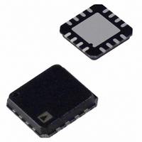
ADL5534ACPZ-R7 Analog Devices Inc, ADL5534ACPZ-R7 Datasheet

ADL5534ACPZ-R7
Specifications of ADL5534ACPZ-R7
Related parts for ADL5534ACPZ-R7
ADL5534ACPZ-R7 Summary of contents
Page 1
FEATURES Fixed gain Operation up to 500 MHz Input/output internally matched to 50 Ω Integrated bias control circuit OIP3 of 40 dBm at 70 MHz P1dB of 20.4 dBm at 70 MHz Noise figure of 2.5 dB ...
Page 2
ADL5534 TABLE OF CONTENTS Features .............................................................................................. 1 Functional Block Diagram .............................................................. 1 General Description ......................................................................... 1 Revision History ............................................................................... 2 Specifications ..................................................................................... 3 Typical Scattering Parameters ..................................................... 4 Absolute Maximum Ratings ............................................................ 5 ESD Caution .................................................................................. 5 Pin Configuration and ...
Page 3
SPECIFICATIONS VPOS = 5 V and T = 25°C, unless otherwise noted. A Table 1. Parameter Conditions OVERALL FUNCTION Frequency Range Gain (S21) 190 MHz Input Return Loss (S11) 190 MHz Output Return Loss (S22) 190 MHz Reverse Isolation (S12) ...
Page 4
ADL5534 TYPICAL SCATTERING PARAMETERS VPOS = 5 V and T = 25°C; the effects of the test fixture have been de-embedded up to the pins of the device. A Table 2. S11 Freq. (MHz) Magnitude (dB) Angle (°) 20 −22.72 ...
Page 5
ABSOLUTE MAXIMUM RATINGS Table 3. Parameter Supply Voltage on RFOUT1, RFOUT2 Input Power on RFIN1, RFIN2 Internal Power Dissipation (Paddle Soldered) θ (Junction-to-Air) JA Maximum Junction Temperature Operating Temperature Range Storage Temperature Range Stresses above those listed under Absolute Maximum ...
Page 6
ADL5534 PIN CONFIGURATION AND FUNCTION DESCRIPTIONS Table 4. Pin Function Descriptions Pin No. Mnemonic 10, 11, 14 RFIN2, RFIN1 7, 12 CLIN2, CLIN1 8, 13 RFOUT2, RFOUT1 Exposed Paddle PIN ...
Page 7
TYPICAL PERFORMANCE CHARACTERISTICS 100 150 200 250 300 FREQUENCY (MHz) Figure 3. Noise Figure, Gain, P1dB, and OIP3 vs. Frequency 21.4 21.2 21.0 20.8 20.6 20.4 ...
Page 8
ADL5534 36.6 37.4 38.2 39.0 39.8 37.0 37.8 38.6 39.4 OIP3 (dBm) Figure 9. OIP3 Distribution at 190 MHz 100 19.0 19.4 19.8 ...
Page 9
BASIC CONNECTIONS Table 5. Recommended Components for Basic Connections Frequency 20 MHz to 500 MHz The basic connections for operating the ADL5534 are shown in Figure 15. Recommended components are listed in Table 5. The inputs and outputs should be ...
Page 10
ADL5534 ADT2-1T-1P+ RFIN USING BALUNS TO COMBINE BOTH AMPLIFIERS INTO A SINGLE AMPLIFIER The ADL5534 is ideal for use in a balanced amplifier confi- guration. To accomplish this, flux-coupled RF transformers with a 2:1 impedance ratio can be used for ...
Page 11
RFIN 3 10nF 4 ADC DRIVING APPLICATION The ADL5534 is a high linearity, fixed gain IF amplifier suitable for use as an ADC driver. The ADL5534 has a differential input and output impedance of 100 Ω. A flux-coupled ...
Page 12
ADL5534 SOLDERING INFORMATION AND RECOMMENDED PCB LAND PATTERN Figure 22 shows the recommended land pattern for ADL5534. To minimize thermal impedance, the exposed paddle on the package underside should be soldered down to a ground plane. If multiple ground layers ...
Page 13
EVALUATION BOARD Figure 23 shows the schematic for the ADL5534 evaluation board. The board is powered by a single 5 V supply. The components used on the board are listed in Table 6. Transformers (T1 and T2) are provided so ...
Page 14
ADL5534 Figure 24. Evaluation Board Layout (Top) Figure 25. Evaluation Board Layout (Bottom) Rev Page ...
Page 15
... OUTLINE DIMENSIONS PIN 1 INDICATOR 12° MAX 1.00 0.85 0.80 ORDERING GUIDE Model Temperature Range 1 ADL5534ACPZ-R7 −40°C to +85°C 1 ADL5534ACPZ-R2 −40°C to +85°C 1 ADL5534-EVALZ RoHS Compliant Part. 5.00 BSC SQ 0.60 MAX 0.80 BSC TOP 4.75 VIEW BSC SQ 0.75 0.60 0.50 ...
Page 16
ADL5534 NOTES ©2008 Analog Devices, Inc. All rights reserved. Trademarks and registered trademarks are the property of their respective owners. D06836-0-6/08(0) Rev Page ...


