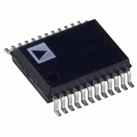
ADE7755ARSZRL Analog Devices Inc, ADE7755ARSZRL Datasheet - Page 6

ADE7755ARSZRL
Manufacturer Part Number
ADE7755ARSZRL
Description
Energy Metering IC With Pulse Output
Manufacturer
Analog Devices Inc
Datasheet
1.ADE7755ARSZRL.pdf
(20 pages)
Specifications of ADE7755ARSZRL
Input Impedance
390 KOhm
Measurement Error
0.1%
Voltage - I/o High
2.4V
Voltage - I/o Low
0.8V
Current - Supply
3mA
Voltage - Supply
4.75 V ~ 5.25 V
Operating Temperature
-40°C ~ 85°C
Mounting Type
Surface Mount
Package / Case
24-SSOP (0.200", 5.30mm Width)
Meter Type
Single Phase
Lead Free Status / RoHS Status
Lead free / RoHS Compliant
For Use With
EVAL-ADE7755ZEB - BOARD EVALUATION FOR AD7755
Lead Free Status / RoHS Status
Lead free / RoHS Compliant
Available stocks
Company
Part Number
Manufacturer
Quantity
Price
Company:
Part Number:
ADE7755ARSZRL
Manufacturer:
FREESCALE
Quantity:
430
ADE7755
PIN CONFIGURATION AND FUNCTION DESCRIPTIONS
Table 4. Pin Function Descriptions
Pin No.
1
2
3
4, 19
5, 6
7, 8
9
10
11
12
13, 14
15, 16
Mnemonic
DV
AC/DC
AV
NC
V1P, V1N
V2N, V2P
RESET
REF
AGND
SCF
S1, S0
G1, G0
DD
DD
IN/OUT
Description
Digital Power Supply. This pin provides the supply voltage for the digital circuitry in the ADE7755. The supply
voltage should be maintained at 5 V ± 5% for specified operation. This pin should be decoupled with a 10 μF
capacitor in parallel with a ceramic 100 nF capacitor.
High-Pass Filter Select. This logic input is used to enable the HPF in Channel 1 (current channel). A Logic 1 on
this pin enables the HPF. The associated phase response of this filter is internally compensated over a
frequency range of 45 Hz to 1 kHz. The HPF should be enabled in power metering applications.
Analog Power Supply. This pin provides the supply voltage for the analog circuitry in the ADE7755. The supply
should be maintained at 5 V ± 5% for specified operation. Every effort should be made to minimize power
supply ripple and noise at this pin by the use of proper decoupling. This pin should be decoupled to AGND
with a 10 μF capacitor in parallel with a ceramic 100 nF capacitor.
No Connect.
Analog Inputs for Channel 1 (Current Channel). These inputs are fully differential voltage inputs with a
maximum differential signal level of ±470 mV for specified operation. Channel 1 also has a PGA, and the gain
selections are outlined in Table 5. The maximum signal level at these pins is ±1 V with respect to AGND. Both
inputs have internal ESD protection circuitry. An overvoltage of ±6 V can be sustained on these inputs without
risk of permanent damage.
Negative and Positive Inputs for Channel 2 (Voltage Channel). These inputs provide a fully differential input pair
with a maximum differential input voltage of ±660 mV for specified operation. The maximum signal level at
these pins is ±1 V with respect to AGND. Both inputs have internal ESD protection circuitry, and an overvoltage
of ±6 V can be sustained on these inputs without risk of permanent damage.
Reset Pin. A logic low on this pin holds the ADCs and digital circuitry in a reset condition.
Bringing this pin logic low clears the ADE7755 internal registers.
This pin provides access to the on-chip voltage reference. The on-chip reference has a nominal value of
2.5 V ± 8% and a typical temperature coefficient of 30 ppm/°C. An external reference source may also be
connected at this pin. In either case, this pin should be decoupled to AGND with a 1 μF ceramic capacitor and
a 100 nF ceramic capacitor.
This pin provides the ground reference for the analog circuitry in the ADE7755, that is, the ADCs and reference.
This pin should be tied to the analog ground plane of the PCB. The analog ground plane is the ground reference
for all analog circuitry, for example, antialiasing filters and current and voltage transducers. For good noise
suppression, the analog ground plane should be connected to the digital ground plane at one point only. A
star ground configuration helps to keep noisy digital currents away from the analog circuits.
Select Calibration Frequency. This logic input is used to select the frequency on the calibration output, CF.
Table 8 shows how the calibration frequencies are selected.
These logic inputs are used to select one of four possible frequencies for the digital-to-frequency conversion.
This offers the designer greater flexibility when designing the energy meter. See the Selecting a Frequency for
an Energy Meter Application section.
These logic inputs are used to select one of four possible gains for Channel 1, that is, V1. The possible gains
are 1, 2, 8, and 16. See the Analog Inputs section.
REF
RESET
AC/DC
AGND
IN/OUT 10
DV
AV
SCF
V1N
V2N
V1P
V2P
NC
DD
DD
Figure 3. Pin Configuration
11
12
1
2
3
4
5
6
7
8
9
NC = NO CONNECT
Rev. A | Page 6 of 20
(Not to Scale)
ADE7755
TOP VIEW
24
23
22
21
20
19
18
17
16
15
14
13
F1
F2
CF
DGND
REVP
NC
CLKOUT
CLKIN
G0
G1
S0
S1


