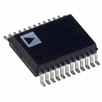
ADE7755ARSZRL Analog Devices Inc, ADE7755ARSZRL Datasheet

ADE7755ARSZRL
Specifications of ADE7755ARSZRL
Available stocks
Related parts for ADE7755ARSZRL
ADE7755ARSZRL Summary of contents
Page 1
FEATURES High accuracy, surpasses 50 Hz/60 Hz IEC 687/IEC 1036 Less than 0.1% error over a dynamic range of 500 to 1 Supplies active power on the frequency outputs, F1 and F2 High frequency output CF is intended for calibration ...
Page 2
ADE7755 TABLE OF CONTENTS Features .............................................................................................. 1 General Description ......................................................................... 1 Functional Block Diagram .............................................................. 1 Revision History ............................................................................... 2 Specifications ..................................................................................... 3 Timing Characteristics ................................................................ 4 Absolute Maximum Ratings ............................................................ 5 ESD Caution .................................................................................. 5 Pin Configuration and Function ...
Page 3
SPECIFICATIONS ± 5%, AGND = DGND = 0 V, on-chip reference, CLKIN = 3.58 MHz Table 1. Parameter 1, 2 ACCURACY 1 Measurement Error on Channel 1 Gain = 1 Gain ...
Page 4
ADE7755 Parameter POWER SUPPLY See the Terminology section. 2 See the Typical Performance Characteristics section for the plots. 3 Sample tested during initial release and after any redesign or process change ...
Page 5
ABSOLUTE MAXIMUM RATINGS T = 25°C, unless otherwise noted. A Table 3. Parameter AV to AGND DGND Analog Input Voltage to AGND V1P, V1N, V2P, and V2N Reference Input Voltage to ...
Page 6
ADE7755 PIN CONFIGURATION AND FUNCTION DESCRIPTIONS Table 4. Pin Function Descriptions Pin No. Mnemonic Description 1 DV Digital Power Supply. This pin provides the supply voltage for the digital circuitry in the ADE7755. The supply DD voltage should be maintained ...
Page 7
Pin No. Mnemonic Description 17 CLKIN An external clock can be provided at this logic input. Alternatively, a parallel resonant AT crystal can be connected across CLKIN and CLKOUT to provide a clock source for the ADE7755. The clock frequency ...
Page 8
ADE7755 TYPICAL PERFORMANCE CHARACTERISTICS 0.5 –40°C 0.4 0.3 0.2 0.1 +25°C 0 –0.1 +85°C –0.2 –0 GAIN = 1 –0.4 ON-CHIP REFERENCE –0.5 0.01 0.1 1 FULL-SCALE CURRENT (%) Figure 4. Error Reading ...
Page 9
PF = 0.5 GAIN = 8 0.6 ON-CHIP REFERENCE –40° 0.5 0.4 0.2 +25° +25° 0.5 –0.2 –0.4 +85° 0.5 –0.6 –0.8 0.01 0.1 1 FULL-SCALE CURRENT (%) Figure ...
Page 10
ADE7755 16 DISTRIBUTION CHARACTERISTICS NUMBER POINTS: 101 14 MINIMUM: –9.78871 GAIN = 1 MAXIMUM: 7.2939 TEMPERATURE = 25°C MEAN: –1.73203 12 STD. DEV: 3.61157 –15 –9 –3 3 CH1 OFFSET (mV) Figure 16. Channel ...
Page 11
TERMINOLOGY Measurement Error The error associated with the energy measurement made by the ADE7755 is defined by the following formula: = Percentage Error Energy Registered by the ADE 7755 True Energy Phase Error Between Channels The high-pass filter (HPF) in ...
Page 12
ADE7755 THEORY OF OPERATION The two ADCs of the ADE7755 digitize the voltage signals from the current and voltage transducers. These ADCs are 16-bit, second-order Σ-Δ with an oversampling rate of 900 kHz. This analog input structure greatly simplifies transducer ...
Page 13
NONSINUSOIDAL VOLTAGE AND CURRENT The active power calculation method also holds true for non- sinusoidal current and voltage waveforms. All voltage and current waveforms in practical applications have some harmonic content. Using the Fourier Transform operation, instantaneous voltage and current ...
Page 14
ADE7755 Channel 2 (Voltage Channel) The output of the line voltage transducer is connected to the ADE7755 at this analog input. Channel fully differential voltage input. The maximum peak differential signal on Channel 2 is ±660 mV. ...
Page 15
HPF and Offset Effects Figure 29 shows the effect of offsets on the active power calculation. An offset on Channel 1 and Channel 2 contributes a dc component after multiplication. Because the dc component is extracted by the LPF, it ...
Page 16
ADE7755 DIGITAL-TO- FREQUENCY V MULTIPLIER DIGITAL-TO- LPF FREQUENCY I LPF TO EXTRACT REAL POWER (DC TERM) V × cos(2ωt) ATTENUATED BY LPF ω 0 2ω FREQUENCY (RAD/s) INSTANTANEOUS ACTIVE POWER SIGNAL (FREQUENCY DOMAIN) Figure 32. Active Power-to-Frequency Conversion ...
Page 17
TRANSFER FUNCTION Frequency Outputs F1 and F2 The ADE7755 calculates the product of two voltage signals (on Channel 1 and Channel 2) and then low-pass filters this product to extract active power information. This active power information is then converted ...
Page 18
ADE7755 Table 8. Maximum Output Frequency on CF SCF ...
Page 19
NO LOAD THRESHOLD The ADE7755 also includes a no load threshold and start-up current feature that eliminates any creep effects in the meter. The ADE7755 is designed to issue a minimum output frequency in all modes except when SCF = ...
Page 20
ADE7755 OUTLINE DIMENSIONS 2.00 MAX 0.05 MIN COPLANARITY 0.10 ORDERING GUIDE Model Temperature Range 1 ADE7755ARSZ −40°C to +85°C 1 ADE7755ARSRLZ −40°C to +85°C EVAL-ADE7755EBZ 1 −40°C to +85° RoHS Compliant Part. ©2002–2009 Analog Devices, Inc. All ...


