ADCMP564BRQ Analog Devices Inc, ADCMP564BRQ Datasheet - Page 12
ADCMP564BRQ
Manufacturer Part Number
ADCMP564BRQ
Description
HIGH SPEED COMPARATOR
Manufacturer
Analog Devices Inc
Type
with Latchr
Datasheet
1.ADCMP564BRQZ.pdf
(16 pages)
Specifications of ADCMP564BRQ
Rohs Compliant
NO
Number Of Elements
2
Output Type
Complementary, Differential, ECL, Open-Emitter
Voltage - Supply
±4.75 V ~ 5.25 V
Mounting Type
Surface Mount
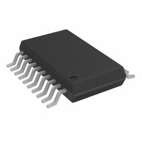
Package / Case
20-SSOP (0.154", 3.91mm Width)
Lead Free Status / RoHS Status
Contains lead / RoHS non-compliant
For Use With
EVAL-ADCMP564BRQZ - BOARD EVALUATION ADCMP564BRQZ
Lead Free Status / RoHS Status
Contains lead / RoHS non-compliant


ADCMP563/ADCMP564
Propagation delay dispersion is important in critical timing
applications such as ATE, bench instruments, and nuclear
instrumentation. Overdrive dispersion is defined as the varia-
tion in propagation delay as the input overdrive conditions are
changed (Figure 21). For the ADCMP563/ADCMP564, over-
drive dispersion is typically 75 ps as the overdrive is changed
from 100 mV to 1.5 V. This specification applies for both
positive and negative overdrive because the ADCMP563 and
the ADCMP564 have equal delays for positive and negative
going inputs.
COMPARATOR HYSTERESIS
The addition of hysteresis to a comparator is often useful in a
noisy environment, or where it is not desirable for the compar-
ator to toggle between states when the input signal is at the
switching threshold. The transfer function for a comparator
with hysteresis is shown in Figure 22. If the input voltage
approaches the threshold from the negative direction, the
comparator switches from 0 to 1 when the input crosses +V
The new switching threshold becomes −V
remains in a 1 state until the threshold −V
coming from the positive direction. In this manner, noise
centered on 0 V input does not cause the comparator to switch
states unless it exceeds the region bounded by ±V
The customary technique for introducing hysteresis into a
comparator uses positive feedback from the output back to the
input. A limitation of this approach is that the amount of
hysteresis varies with the output logic levels, resulting in
hysteresis that can be load dependent and is not symmetrical
about the threshold. The external feedback network can also
introduce significant parasitics, which reduce high speed
performance and can induce oscillation in some cases.
In the ADCMP564, hysteresis is generated through the
programmable hysteresis pin. A resistor from the HYS pin to
GND creates a current into the part that is used to generate
hysteresis. Hysteresis generated in this manner is independent
of output swing and is symmetrical around the trip point. The
hysteresis vs. resistance curve is shown in Figure 23.
INPUT VOLTAGE
Q OUTPUT
Figure 21. Propagation Delay Dispersion
1.5V OVERDRIVE
20mV OVERDRIVE
V
REF
DISPERSION
H
H
± V
/2. The comparator
/2 is crossed while
OS
H
/2.
H
Rev. B | Page 12 of 16
/2.
A current may be sourced into the HYS pin. The pin is biased
approximately 1 V below AGND and has a 3 kΩ series
resistance. The relationship between the current applied to the
HYS pin and the resulting hysteresis is shown in Figure 19.
MINIMUM INPUT SLEW RATE REQUIREMENT
As for all high speed comparators, a minimum slew rate must
be met to ensure that the device does not oscillate as the input
crosses the threshold. This oscillation is due in part to the high
input bandwidth of the comparator and the parasitics of the
package. ADI recommends a slew rate of 1 V/μs or faster to
ensure a clean output transition. If slew rates less than 1 V/μs
are used, hysteresis can be added to prevent the oscillation.
160
140
120
100
80
60
40
20
0
0
50
Figure 22. Comparator Hysteresis Transfer Function
Figure 23. Comparator Hysteresis vs. R
–V
40
2
H
30
0V
R
OUTPUT
HYS
(kΩ)
20
+V
2
H
HYS
10
INPUT
1
0
Related parts for ADCMP564BRQ
Image
Part Number
Description
Manufacturer
Datasheet
Request
R

Part Number:
Description:
Agilent Adcm-2650-0001 Portrait Vga Resolution Cmos Camera Module - Agilent Hewlett-packard
Manufacturer:
Avago Technologies
Datasheet:

Part Number:
Description:
±1.7g Dual-Axis IMEMS Accelerometer Evaluation Board
Manufacturer:
Analog Devices Inc
Datasheet:

Part Number:
Description:
Inertial Sensor Evaluation System
Manufacturer:
Analog Devices Inc
Datasheet:
Part Number:
Description:
Manufacturer:
Analog Devices Inc
Datasheet:
Part Number:
Description:
Manufacturer:
Analog Devices Inc
Datasheet:
Part Number:
Description:
Manufacturer:
Analog Devices Inc
Datasheet:
Part Number:
Description:
Manufacturer:
Analog Devices Inc
Datasheet:
Part Number:
Description:
Manufacturer:
Analog Devices Inc
Datasheet:
Part Number:
Description:
Manufacturer:
Analog Devices Inc
Datasheet:
Part Number:
Description:
Manufacturer:
Analog Devices Inc
Datasheet:
Part Number:
Description:
Manufacturer:
Analog Devices Inc
Datasheet:
Part Number:
Description:
Manufacturer:
Analog Devices Inc
Datasheet:
Part Number:
Description:
Manufacturer:
Analog Devices Inc
Datasheet: