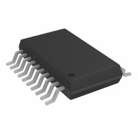
ADCMP564BRQ Analog Devices Inc, ADCMP564BRQ Datasheet - Page 10

ADCMP564BRQ
Manufacturer Part Number
ADCMP564BRQ
Description
HIGH SPEED COMPARATOR
Manufacturer
Analog Devices Inc
Type
with Latchr
Datasheet
1.ADCMP564BRQZ.pdf
(16 pages)
Specifications of ADCMP564BRQ
Rohs Compliant
NO
Number Of Elements
2
Output Type
Complementary, Differential, ECL, Open-Emitter
Voltage - Supply
±4.75 V ~ 5.25 V
Mounting Type
Surface Mount
Package / Case
20-SSOP (0.154", 3.91mm Width)
Lead Free Status / RoHS Status
Contains lead / RoHS non-compliant
For Use With
EVAL-ADCMP564BRQZ - BOARD EVALUATION ADCMP564BRQZ
Lead Free Status / RoHS Status
Contains lead / RoHS non-compliant
ADCMP563/ADCMP564
TIMING INFORMATION
Figure 20 shows the compare and latch features of the ADCMP563. Table 4 describes the terms in the diagram.
Table 4. Timing Descriptions
Symbol
t
t
t
t
t
t
t
t
t
V
PDH
PDL
PLOH
PLOL
H
PL
S
R
F
OD
Timing
Input-to-Output High Delay
Input-to-Output Low Delay
Latch Enable to Output High Delay
Latch Enable to Output Low Delay
Minimum Hold Time
Minimum Latch Enable Pulse Width
Minimum Setup Time
Output Rise Time
Output Fall Time
Voltage Overdrive
INPUT VOLTAGE
LATCH ENABLE
LATCH ENABLE
DIFFERENTIAL
Q OUTPUT
Q OUTPUT
V
IN
Description
Propagation delay measured from the time the input signal crosses the reference (± the
input offset voltage) to the 50% point of an output low-to-high transition.
Propagation delay measured from the time the input signal crosses the reference (± the
input offset voltage) to the 50% point of an output high-to-low transition.
Propagation delay measured from the 50% point of the latch enable signal low-to-high
transition to the 50% point of an output low-to-high transition.
Propagation delay measured from the 50% point of the latch enable signal low-to-high
transition to the 50% point of an output high-to-low transition.
Minimum time after the negative transition of the latch enable signal that the input signal
must remain unchanged to be acquired and held at the outputs.
Minimum time the latch enable signal must be high to acquire an input signal change.
Minimum time before the negative transition of the latch enable signal that an input
signal change must be present to be acquired and held at the outputs.
Amount of time required to transition from a low to a high output as measured at the
20% and 80% points.
Amount of time required to transition from a high to a low output as measured at the
20% and 80% points.
Difference between the differential input and reference input voltages.
V
Figure 20. System Timing Diagram
t
S
OD
t
t
PDL
PDH
Rev. B | Page 10 of 16
t
H
t
R
t
F
t
PL
t
t
PLOH
PLOL
50%
V
50%
50%
REF
± V
OS


