ADCMP552BRQ Analog Devices Inc, ADCMP552BRQ Datasheet - Page 5
ADCMP552BRQ
Manufacturer Part Number
ADCMP552BRQ
Description
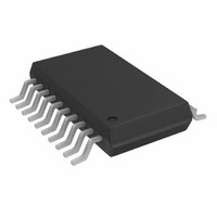
IC,VOLT COMPARATOR,SINGLE,ECL,SSOP,20PIN,PLASTIC
Manufacturer
Analog Devices Inc
Type
with Latchr
Datasheet
1.ADCMP553BRMZ.pdf
(16 pages)
Specifications of ADCMP552BRQ
Number Of Elements
2
Output Type
Complementary, Differential, LVPECL, Open-Emitter, PECL
Voltage - Supply
3.14 V ~ 5.25 V
Mounting Type
Surface Mount
Package / Case
20-SSOP (0.154", 3.91mm Width)
Number Of Elements
1
Input Offset Voltage
10mV
Input Bias Current (typ)
5uA
Response Time
625ps
Single Supply Voltage (typ)
3.3V
Dual Supply Voltage (typ)
Not RequiredV
Supply Current (max)
70@3.3VmA
Power Supply Requirement
Single
Common Mode Rejection Ratio
76dB
Voltage Gain In Db
60dB
Power Supply Rejection Ratio
75dB
Single Supply Voltage (min)
3.135V
Single Supply Voltage (max)
5.25V
Dual Supply Voltage (min)
Not RequiredV
Dual Supply Voltage (max)
Not RequiredV
Power Dissipation
130mW
Operating Temp Range
-40C to 85C
Operating Temperature Classification
Industrial
Mounting
Surface Mount
Pin Count
20
Package Type
QSOP
Lead Free Status / RoHS Status
Contains lead / RoHS non-compliant
For Use With
EVAL-ADCMP552BRQZ - BOARD EVALUATION ADCMP552BRQZ
Lead Free Status / Rohs Status
Not Compliant


ABSOLUTE MAXIMUM RATINGS
Table 2.
Parameter
Supply Voltages
Input Voltages
Output
Temperature
ESD CAUTION
ESD (electrostatic discharge) sensitive device. Electrostatic charges as high as 4000 V readily accumulate on
the human body and test equipment and can discharge without detection. Although this product features
proprietary ESD protection circuitry, permanent damage may occur on devices subjected to high energy
electrostatic discharges. Therefore, proper ESD precautions are recommended to avoid performance
degradation or loss of functionality.
Input Supply Voltage (V
Output Supply Voltage (V
Ground Voltage Differential
Input Common-Mode Voltage
Differential Input Voltage
Input Voltage, Latch Controls
Output Current
Operating Temperature, Ambient
Operating Temperature, Junction
Storage Temperature Range
CCI
CCO
to GND)
to GND)
Rating
−0.5 V to +6.0 V
−0.5 V to +6.0 V
−0.5 V to +0.5 V
−0.5 V to +3.5 V
−4.0 V to +4.0 V
−0.5 V to +5.5 V
30 mA
−40°C to +85°C
125°C
−65°C to +150°C
Rev. 0 | Page 5 of 16
Stresses above those listed under Absolute Maximum Ratings
may cause permanent damage to the device. This is a stress
rating only; functional operation of the device at these or any
other conditions above those indicated in the operational
sections of this specification is not implied. Exposure to
absolute maximum rating conditions for extended periods may
affect device reliability.
THERMAL CONSIDERATIONS
The ADCMP551 16-lead QSOP package has a θ
ambient thermal resistance) of 104°C/W in still air.
The ADCMP552 20-lead QSOP package has a θ
ambient thermal resistance) of 80°C/W in still air.
The ADCMP553 8-lead MSOP package has a θ
ambient thermal resistance) of 130°C/W in still air.
ADCMP551/ADCMP552/ADCMP553
JA
JA
JA
(junction-to-
(junction-to-
(junction-to-
Related parts for ADCMP552BRQ
Image
Part Number
Description
Manufacturer
Datasheet
Request
R

Part Number:
Description:
Agilent Adcm-2650-0001 Portrait Vga Resolution Cmos Camera Module - Agilent Hewlett-packard
Manufacturer:
Avago Technologies
Datasheet:

Part Number:
Description:
±1.7g Dual-Axis IMEMS Accelerometer Evaluation Board
Manufacturer:
Analog Devices Inc
Datasheet:

Part Number:
Description:
Inertial Sensor Evaluation System
Manufacturer:
Analog Devices Inc
Datasheet:
Part Number:
Description:
Manufacturer:
Analog Devices Inc
Datasheet:
Part Number:
Description:
Manufacturer:
Analog Devices Inc
Datasheet:
Part Number:
Description:
Manufacturer:
Analog Devices Inc
Datasheet:
Part Number:
Description:
Manufacturer:
Analog Devices Inc
Datasheet:
Part Number:
Description:
Manufacturer:
Analog Devices Inc
Datasheet:
Part Number:
Description:
Manufacturer:
Analog Devices Inc
Datasheet:
Part Number:
Description:
Manufacturer:
Analog Devices Inc
Datasheet:
Part Number:
Description:
Manufacturer:
Analog Devices Inc
Datasheet:
Part Number:
Description:
Manufacturer:
Analog Devices Inc
Datasheet:
Part Number:
Description:
Manufacturer:
Analog Devices Inc
Datasheet: