ADCMP552BRQ Analog Devices Inc, ADCMP552BRQ Datasheet - Page 4
ADCMP552BRQ
Manufacturer Part Number
ADCMP552BRQ
Description
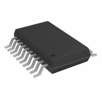
IC,VOLT COMPARATOR,SINGLE,ECL,SSOP,20PIN,PLASTIC
Manufacturer
Analog Devices Inc
Type
with Latchr
Datasheet
1.ADCMP553BRMZ.pdf
(16 pages)
Specifications of ADCMP552BRQ
Number Of Elements
2
Output Type
Complementary, Differential, LVPECL, Open-Emitter, PECL
Voltage - Supply
3.14 V ~ 5.25 V
Mounting Type
Surface Mount
Package / Case
20-SSOP (0.154", 3.91mm Width)
Number Of Elements
1
Input Offset Voltage
10mV
Input Bias Current (typ)
5uA
Response Time
625ps
Single Supply Voltage (typ)
3.3V
Dual Supply Voltage (typ)
Not RequiredV
Supply Current (max)
70@3.3VmA
Power Supply Requirement
Single
Common Mode Rejection Ratio
76dB
Voltage Gain In Db
60dB
Power Supply Rejection Ratio
75dB
Single Supply Voltage (min)
3.135V
Single Supply Voltage (max)
5.25V
Dual Supply Voltage (min)
Not RequiredV
Dual Supply Voltage (max)
Not RequiredV
Power Dissipation
130mW
Operating Temp Range
-40C to 85C
Operating Temperature Classification
Industrial
Mounting
Surface Mount
Pin Count
20
Package Type
QSOP
Lead Free Status / RoHS Status
Contains lead / RoHS non-compliant
For Use With
EVAL-ADCMP552BRQZ - BOARD EVALUATION ADCMP552BRQZ
Lead Free Status / Rohs Status
Not Compliant


ADCMP551/ADCMP552/ADCMP553
Parameter
AC PERFORMANCE (continued)
POWER SUPPLY (ADCMP551/ADCMP552)
POWER SUPPLY (ADCMP553)
HYSTERESIS (ADCMP552 Only)
1
Equivalent input rise time bandwidth assumes a first order input response and is calculated by the following formula: BW
where tr
Equivalent Input Rise Time Bandwidth
Maximum Toggle Rate
Minimum Pulse Width
RMS Random Jitter
Unit-to-Unit Propagation Delay Skew
Input Supply Current
Output Supply Current
Output Supply Current
Input Supply Voltage
Output Supply Voltage
Positive Supply Differential
Power Dissipation
Power Dissipation
DC Power Supply Rejection Ratio—V
DC Power Supply Rejection Ratio—V
Positive Supply Current
Positive Supply Current
Positive Supply Voltage
Power Dissipation
Power Dissipation
DC Power Supply Rejection Ratio—V
Programmable Hysteresis
IN
is the 20/80 input transition time applied to the comparator and tr
CCI
CCO
CC
1
Symbol
BW
PW
I
I
V
V
V
P
PSRR
PSRR
I
V
P
PSRR
VCCI
VCCO
VCC
D
D
CCI
CCO
CCO
CC
EQ
MIN
− V
VCCI
VCCO
VCC
CCI
Conditions
0 V to 1 V swing, 2 V/ns
>50% output swing
∆t
V
500 MHz, 50% duty cycle
@ 3.3 V
@ 3.3 V without load
@ 3.3 V with load
Dual
Dual
Dual, without load
Dual, with load
@ 3.3 V without load
@ 3.3 V with load
Dual
Dual, without load
Dual, with load
OD
Rev. 0 | Page 4 of 16
PD
= 250 mV, 1.3 V/ns,
< 25 ps
COMP
is the effective transition time as digitized by the comparator input.
Min
8
3
40
3.135
3.135
–0.2
40
90
3.135
0
EQ
= .22/√ (tr
Typ
750
800
700
1.1
50
12
5
55
3.3
3.3
55
110
75
85
9
35
3.3
30
60
70
COMP
2
- tr
Max
17
9
70
5.25
5.25
+2.3
75
130
13
42
5.25
42
75
40
IN
2
),
Unit
MHz
MHz
ps
ps
ps
mA
mA
mA
V
V
V
mW
mW
dB
dB
mA
mA
V
mW
mW
dB
mV
Related parts for ADCMP552BRQ
Image
Part Number
Description
Manufacturer
Datasheet
Request
R

Part Number:
Description:
Agilent Adcm-2650-0001 Portrait Vga Resolution Cmos Camera Module - Agilent Hewlett-packard
Manufacturer:
Avago Technologies
Datasheet:

Part Number:
Description:
±1.7g Dual-Axis IMEMS Accelerometer Evaluation Board
Manufacturer:
Analog Devices Inc
Datasheet:

Part Number:
Description:
Inertial Sensor Evaluation System
Manufacturer:
Analog Devices Inc
Datasheet:
Part Number:
Description:
Manufacturer:
Analog Devices Inc
Datasheet:
Part Number:
Description:
Manufacturer:
Analog Devices Inc
Datasheet:
Part Number:
Description:
Manufacturer:
Analog Devices Inc
Datasheet:
Part Number:
Description:
Manufacturer:
Analog Devices Inc
Datasheet:
Part Number:
Description:
Manufacturer:
Analog Devices Inc
Datasheet:
Part Number:
Description:
Manufacturer:
Analog Devices Inc
Datasheet:
Part Number:
Description:
Manufacturer:
Analog Devices Inc
Datasheet:
Part Number:
Description:
Manufacturer:
Analog Devices Inc
Datasheet:
Part Number:
Description:
Manufacturer:
Analog Devices Inc
Datasheet:
Part Number:
Description:
Manufacturer:
Analog Devices Inc
Datasheet: