ADC0808S250HW/C1:5 NXP Semiconductors, ADC0808S250HW/C1:5 Datasheet
ADC0808S250HW/C1:5
Specifications of ADC0808S250HW/C1:5
935286577151
935286577551
ADC0808S250HW/C1
ADC0808S250HW/C1-S
ADC0808S250HW/C1-S
Available stocks


Related parts for ADC0808S250HW/C1:5


ADC0808S250HW/C1:5 Summary of contents
Page 1
ADC0808S125/250 Single 8-bit ADC 125 MHz or 250 MHz Rev. 03 — 24 February 2009 1. General description The ADC0808S is a differential, high-speed, 8-bit Analog-to-Digital Converter (ADC) optimized for telecommunication transmission control systems and tape drive applications. ...
Page 2
... NXP Semiconductors I Optical networking I Wireless Local Area Network (WLAN) infrastructure I Tape drive applications 4. Ordering information Table 1. Ordering information Type number Sampling frequency (MHz) ADC0808S125HW/C1 125 ADC0808S250HW/C1 250 5. Block diagram FSIN/ REFSEL Fig 1. ADC0808S125_ADC0808S250_3 Product data sheet Package Name Description HTQFP48 plastic thermal enhanced thin quad flat package; ...
Page 3
... NXP Semiconductors 6. Pinning information 6.1 Pinning Fig 2. 6.2 Pin description Table 2. Symbol OGND1 D3 i.c. V CCO1(1V8) D4 i.c. OGND2 D5 i.c. V CCO2(1V8) D6 i.c. V CCO3(1V8) D7 ADC0808S125_ADC0808S250_3 Product data sheet 1 OGND1 CCO1(1V8 i.c. 6 ADC0808S OGND2 i. CCO2(1V8 i.c. 12 Pin configuration Pin description [1] Pin Type Description ...
Page 4
... NXP Semiconductors Table 2. Symbol i.c. OGND3 CCS i.c. CE_N IR OTC DGND1 V CCD1(1V8) n.c. n.c. CCSSEL NC1V8 AGND1 CMADC FSIN/REFSEL AGND2 INN IN V CCA1(3V3) i.c. CLKSEL CLK+ CLK DEL0 DEL1 D0 i.c. V CCO4(1V8) D1 i.c. OGND4 D2 i.c. DGND [1] See ADC0808S125_ADC0808S250_3 Product data sheet Pin description … ...
Page 5
... NXP Semiconductors Table 3. Type I O I(CMOS) O(CMOS Functional description 7.1 CMOS/LVDS clock input The circuit has two clock inputs CLK+ and CLK , with two modes of operation: • LVDS mode: CLK+ and CLK inputs are at differential LVDS levels. An external resistor of between 80 Fig 3. LVDS clock input • ...
Page 6
... NXP Semiconductors Table 4. Pin CLKSEL HIGH or not connected LOW 7.2 Digital output coding The digital outputs are 1.8 V CMOS compatible. The data output format can be either binary or 2’s complement. Table 2 i(p-p) Code Underfl 127 : 254 255 Overflow The in-range CMOS output pin IR will be HIGH during normal operation. When the ADC input reaches either positive or negative full-scale, the IR output will be LOW ...
Page 7
... NXP Semiconductors 7.3 Timing output Fig 5. 7.4 Timing complete conversion signal The ADC0808S generates an adjustable clock output signal on pin CCS called Complete Conversion Signal, which can be used to control the acquisition of converted output data to the digital circuit connected to the ADC0808S output data bus. ...
Page 8
... NXP Semiconductors Fig 6. 7.5 Full-scale input selection The ADC0808S has an internal reference circuit which can be overruled by an external reference voltage. This can be done with the full-scale reference voltage (V according to The ADC provides the required common-mode voltage on pin CMADC. In case of internal regulation, the regulator output voltage on pin CMADC is 0.95 V. ...
Page 9
... NXP Semiconductors V O(cm) (V) Fig 7. V i(p-p)(max) (V) Fig 8. IN INN FSIN/REFSEL CMADC a. External reference voltage applied Fig 9. ADC full-scale input selection ADC0808S125_ADC0808S250_3 Product data sheet 1.1 1.0 0.9 0.8 0.7 0 1.1 ADC common-mode output voltage V 2.2 2.1 2.0 1.9 1.8 1.0 1 ...
Page 10
... NXP Semiconductors 8. Limiting values Table 10. In accordance with the Absolute Maximum Rating System (IEC 60134). Symbol V CCA V CCD V CCO V i(IN) V i(INN) V i(CLK) T stg T amb Thermal characteristics Table 11. Symbol R th(j-a) R th(j-c) [1] In compliance with JEDEC test board, in free air. 10. Static characteristics Table 12. ...
Page 11
... NXP Semiconductors Table 12. Static characteristics CCA CCD + amb i( CCA CCD CCO Symbol Parameter V input differential threshold voltage |V idth I input current I 1.8 V CMOS clock input; see Figure 4 V LOW-level input voltage IL V HIGH-level input voltage IH I LOW-level input current ...
Page 12
... NXP Semiconductors 11. Dynamic characteristics Table 13. Dynamic characteristics CCA CCD + amb i( CCA CCD CCO Symbol Parameter Clock timing input: pins CLK+ and CLK f minimum clock frequency clk(min) f maximum clock frequency clk(max) t clock pulse width w(clk) Timing output: pins and IR ...
Page 13
... NXP Semiconductors Table 13. Dynamic characteristics CCA CCD + amb i( CCA CCD CCO Symbol Parameter SFDR spurious free dynamic range IMD2 second-order intermodulation distortion IMD3 third-order intermodulation distortion [1] Output data acquisition: the output data is available after the maximum delay of t [2] The 3 dB analog bandwidth is determined by the 3 dB reduction in the reconstructed output, the input being a full-scale sine wave ...
Page 14
... NXP Semiconductors Fig 10. Single tone spectrum of full-scale input sine wave of frequency f Remark: P which include random noise, non-linearities, sampling time errors, and quantization noise. 12.2.1 Signal-to-Noise And Distortion (SINAD) SINAD is the ratio of the output signal power to the noise plus distortion power for a given ...
Page 15
... NXP Semiconductors P harmonics P = signal The value usually 6 (THD is calculated based on the first 5 harmonics). 12.2.4 Signal-to-Noise ratio (S/N) S/N is the ratio of the output signal power to the noise power, excluding the harmonics and the DC component 12.2.5 Spurious Free Dynamic Range (SFDR) The SFDR value specifies the available signal range as the spectral distance between the ...
Page 16
... NXP Semiconductors The total intermodulation distortion is given by: IMD dB where: P intermod where P signal ADC0808S125_ADC0808S250_3 Product data sheet P intermod = 10log --------------------- - 10 P signal – – – the power in the intermodulation component Rev. 03 — 24 February 2009 ADC0808S125/250 Single 8-bit ADC 125 MHz or 250 MHz – ...
Page 17
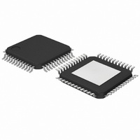
... NXP Semiconductors 13. Package outline HTQFP48: plastic thermal enhanced thin quad flat package; 48 leads; body mm; exposed die pad y exposed die pad side pin 1 index DIMENSIONS (mm are the original dimensions) A UNIT max. 0.15 1.05 0.27 mm 1.2 0.25 0.05 0.95 0.17 Note 1. Plastic or metal protrusions of 0.25 mm maximum per side are not included. ...
Page 18
... NXP Semiconductors 14. Soldering of SMD packages This text provides a very brief insight into a complex technology. A more in-depth account of soldering ICs can be found in Application Note AN10365 “Surface mount reflow soldering description” . 14.1 Introduction to soldering Soldering is one of the most common methods through which packages are attached to Printed Circuit Boards (PCBs), to form electrical circuits ...
Page 19
... NXP Semiconductors 14.4 Reflow soldering Key characteristics in reflow soldering are: • Lead-free versus SnPb soldering; note that a lead-free reflow process usually leads to higher minimum peak temperatures (see reducing the process window • Solder paste printing issues including smearing, release, and adjusting the process window for a mix of large and small components on one board • ...
Page 20
... NXP Semiconductors Fig 13. Temperature profiles for large and small components For further information on temperature profiles, refer to Application Note AN10365 “Surface mount reflow soldering description” . ADC0808S125_ADC0808S250_3 Product data sheet maximum peak temperature = MSL limit, damage level temperature minimum peak temperature ...
Page 21
... NXP Semiconductors 15. Revision history Table 16. Revision history Document ID ADC0808S125_ADC0808S250_3 Modifications: ADC0808S125_ADC0808S250_2 TDA9917_1 ADC0808S125_ADC0808S250_3 Product data sheet Release date Data sheet status 20090224 Product data sheet • Table 13 updated. 20081007 Product data sheet 20060609 Objective data sheet Rev. 03 — 24 February 2009 ...
Page 22
... Right to make changes — NXP Semiconductors reserves the right to make changes to information published in this document, including without limitation specifications and product descriptions, at any time and without notice ...
Page 23
... NXP Semiconductors 18. Contents 1 General description . . . . . . . . . . . . . . . . . . . . . . 1 2 Features . . . . . . . . . . . . . . . . . . . . . . . . . . . . . . . 1 3 Applications . . . . . . . . . . . . . . . . . . . . . . . . . . . . 1 4 Ordering information . . . . . . . . . . . . . . . . . . . . . 2 5 Block diagram . . . . . . . . . . . . . . . . . . . . . . . . . . 2 6 Pinning information . . . . . . . . . . . . . . . . . . . . . . 3 6.1 Pinning . . . . . . . . . . . . . . . . . . . . . . . . . . . . . . . 3 6.2 Pin description . . . . . . . . . . . . . . . . . . . . . . . . . 3 7 Functional description . . . . . . . . . . . . . . . . . . . 5 7.1 CMOS/LVDS clock input . . . . . . . . . . . . . . . . . . 5 7.2 Digital output coding . . . . . . . . . . . . . . . . . . . . . 6 7.3 Timing output . . . . . . . . . . . . . . . . . . . . . . . . . . 7 7.4 Timing complete conversion signal ...