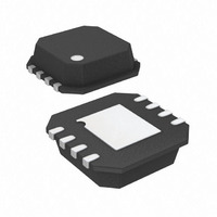
ADA4817-1ACPZ-RL Analog Devices Inc, ADA4817-1ACPZ-RL Datasheet - Page 15

ADA4817-1ACPZ-RL
Manufacturer Part Number
ADA4817-1ACPZ-RL
Description
Hi Speed FET Input Amp
Manufacturer
Analog Devices Inc
Series
FastFET™r
Datasheet
1.ADA4817-1ACPZ-R7.pdf
(24 pages)
Specifications of ADA4817-1ACPZ-RL
Amplifier Type
Voltage Feedback
Number Of Circuits
1
Slew Rate
870 V/µs
Gain Bandwidth Product
410MHz
-3db Bandwidth
1.05GHz
Current - Input Bias
2pA
Voltage - Input Offset
400µV
Current - Supply
19mA
Current - Output / Channel
40mA
Voltage - Supply, Single/dual (±)
5 V ~ 10 V, ±2.5 V ~ 5 V
Operating Temperature
-40°C ~ 105°C
Mounting Type
Surface Mount
Package / Case
8-LFCSP
Lead Free Status / RoHS Status
Lead free / RoHS Compliant
Output Type
-
Lead Free Status / RoHS Status
Lead free / RoHS Compliant
POWER-DOWN OPERATION
The ADA4817-1/ADA4817-2 are equipped with separate
power-down pins ( PD ) pins for each amplifier. This allows the
user the ability to reduce the quiescent supply current when
an amplifier is inactive from 2 mA to 19 mA. The power-down
threshold levels are derived from the voltage applied to the +V
pin. In ±5 V supply application, the enable voltage is greater
than +4 V, and in a ±3 V supply application, the enable voltage
is greater than +2 V. However, the amplifier is powered down
whenever the voltage applied to the PD pin is 3 V below +V
If the PD pin is not to be used, it is best to connect it to the
positive supply.
Table 7. Power-Down Voltage Control
PD Pin
Not active
Active
CAPACITIVE FEEDBACK
Due to package variations and pin-to-pin parasitic between the
single and the dual, the ADA4817-2 has a little more peaking
then the ADA4817-1, especially at a gain of 2. The best way to
tame the peaking is to place a feedback capacitor across the
feedback resistor.
±5 V
>4 V
<2 V
+3 V, −2 V
>2 V
<0 V
S
.
Rev. 0 | Page 15 of 24
S
Figure 43 shows the small signal frequency response of the
ADA4817-2 at a gain of 2 vs. C
the peaking then two other values of 0.5 pF and 1 pF were used
to show how to reduce the peaking or even eliminate it. As
shown in Figure 43, if the power consumption is a factor in
the system, then using a larger feedback capacitor is acceptable
as long as a feedback capacitor is used across it to control the
peaking. However, if the power consumption is not an issue,
then a lower value feedback resistor such as 100 Ω, would not
require any additional feedback capacitance to maintain flatness
and lower peaking.
Figure 43. Small Signal Frequency Response vs. Feedback Capacitor
–3
–6
–9
9
6
3
0
0.1
R
G = 2
V
V
R
F
S
OUT
L
= 10V
= 348Ω
= 100Ω
= 100mV p-p
1
(ADA4817-2)
FREQUENCY (MHz)
ADA4817-1/ADA4817-2
10
C
F
F
. At first no C
= 0.5pF
C
F
= 1pF
100
F
NO C
was used to show
1k
F
10k


