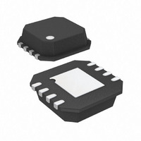
ADA4817-1ACPZ-RL Analog Devices Inc, ADA4817-1ACPZ-RL Datasheet - Page 14

ADA4817-1ACPZ-RL
Manufacturer Part Number
ADA4817-1ACPZ-RL
Description
Hi Speed FET Input Amp
Manufacturer
Analog Devices Inc
Series
FastFET™r
Datasheet
1.ADA4817-1ACPZ-R7.pdf
(24 pages)
Specifications of ADA4817-1ACPZ-RL
Amplifier Type
Voltage Feedback
Number Of Circuits
1
Slew Rate
870 V/µs
Gain Bandwidth Product
410MHz
-3db Bandwidth
1.05GHz
Current - Input Bias
2pA
Voltage - Input Offset
400µV
Current - Supply
19mA
Current - Output / Channel
40mA
Voltage - Supply, Single/dual (±)
5 V ~ 10 V, ±2.5 V ~ 5 V
Operating Temperature
-40°C ~ 105°C
Mounting Type
Surface Mount
Package / Case
8-LFCSP
Lead Free Status / RoHS Status
Lead free / RoHS Compliant
Output Type
-
Lead Free Status / RoHS Status
Lead free / RoHS Compliant
ADA4817-1/ADA4817-2
The voltage error due to I
(though with the ADA4817-1/ADA4817-2 input currents in the
picoamp range, this is likely not a concern). To include common-
mode effects and power supply rejection effects, total V
modeled by
where:
ΔV
PSR is the power supply rejection.
ΔV
conditions.
CMR is the common-mode rejection.
WIDEBAND OPERATION
The ADA4817-1/ADA4817-2 provides excellent performance as a
high speed buffer. Figure 38 shows the circuit used for wideband
characterization for high gains. The impedance at the summing
junction (R
with the amplifier’s input capacitance of 1.5 pF. This pole can
cause peaking and ringing if its frequency is too low. Feedback
resistances of 100 Ω to 400 Ω are recommended, because they
minimize the peaking and they do not degrade the perfor-
mance of the output stage. Peaking in the frequency response
can also be compensated for with a small feedback capacitor
(C
in the noninverting input as shown in Figure 42.
The distortion performance depends on a number of variables:
•
•
•
•
•
The best performance is usually obtained in the G + 1
configuration with no feedback resistance, big output
load resistors, and small board parasitic capacitances.
DRIVING CAPACITIVE LOADS
In general, high speed amplifiers have a difficult time driving
capacitive loads. This is particularly true in low closed-loop
gains, where the phase margin is the lowest. The difficulty
arises because the load capacitance, C
output resistance, R
by the following equation:
V
OS
F
CM
) in parallel with the feedback resistor, or a series resistor
S
nom
is the change in power supply from nominal conditions.
The closed-loop gain of the application
Whether it is inverting or noninverting
Amplifier loading
Signal frequency and amplitude
Board layout
V
f
is the change in common-mode voltage from nominal
P
OS
is the offset voltage specified at nominal conditions.
=
=
2π
F
V
|| R
OS
R
1
O
nom
G
C
) forms a pole in the amplifier’s loop response
L
+
O
, of the amplifier. The pole can be described
Δ
PSR
V
S
b+
+
and I
Δ
CMR
V
CM
b–
is minimized if R
L
, forms a pole with the
S
OS
= R
can be
F
|| R
(11)
(12)
Rev. 0 | Page 14 of 24
G
If this pole occurs too close to the unity-gain crossover point,
the phase margin degrades. This is due to the additional phase
loss associated with the pole.
Note that such capacitance introduces significant peaking in the
frequency response. Larger capacitance values can be driven but
must use a snubbing resistor (R
as shown in Figure 42. Adding a small series resistor, R
creates a zero that cancels the pole introduced by the load
capacitance. Typical values for R
50 Ω. The value is typically based on the circuit requirements.
Figure 42 also shows another way to reduce the effect of the
pole created by the capacitive load (C
(C
Typical capacitor values can range from 0.5 pF to 2 pF.
Figure 43 shows the effect of adding a feedback capacitor
to the frequency response.
THERMAL CONSIDERATIONS
With 10 V power supplies and 19 mA quiescent current, the
ADA4817-1/ADA4817-2 dissipate 190 mW with no load. This
implies that in the LFCSP, whose thermal resistance is 94°C/W
for the ADA4817-1and 64°C/W for the ADA4817-2, the junction
temperature is typically almost 25° higher than the ambient tem-
perature. The ADA4817-1/ADA4817-2 are designed to maintain
a constant bandwidth over temperature; therefore, an initial ramp
up of the current consumption during warm-up is expected. The
V
up to 0.3 mV due to warm-up effects for an ADA4817-1/
ADA4817-2 in a LFCSP on 10 V. The input bias current
increases by a factor of 1.7 for every 10°C rise in temperature.
Heavy loads increase power dissipation and raise the chip
junction temperature as described in the Absolute Maximum
Ratings section. Care should be taken not to exceed the rated
power dissipation of the package.
OS
F
) in the feedback loop parallel to the feedback resistor
temperature drift is below 12 μV/°C; therefore, it can change
V
IN
Figure 42. R
49.9Ω
R
G
10µF
10µF
C
R
F
F
SNUB
+V
–V
or C
S
S
F
SNUB
Used to Reduce Peaking
R
SNUB
0.1µF
SNUB
) at the output of the amplifier,
0.1µF
can range from 10 Ω to
L
) by placing a capacitor
0.1µF
C
L
R
L
V
OUT
SNUB
,


