ADA4817-1ACPZ-RL Analog Devices Inc, ADA4817-1ACPZ-RL Datasheet
ADA4817-1ACPZ-RL
Specifications of ADA4817-1ACPZ-RL


Related parts for ADA4817-1ACPZ-RL


ADA4817-1ACPZ-RL Summary of contents
Page 1
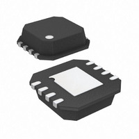
... ADA4817-2 are designed to work in a variety of applications including active filtering and ADC driving. The ADA4817-1 is available × 8-lead LFCSP and the ADA4817-2 is available × 16-lead LFSCP. Both packages feature a low distortion pinout, which improves second harmonic distortion and simplifies the layout of the circuit board ...
Page 2
... ADA4817-1/ADA4817-2 TABLE OF CONTENTS Features .............................................................................................. 1 Applications ....................................................................................... 1 Connection Diagrams ...................................................................... 1 General Description ......................................................................... 1 Revision History ............................................................................... 2 Specifications ..................................................................................... 3 ±5 V Operation ............................................................................. Operation ............................................................................... 4 Absolute Maximum Ratings ............................................................ 5 Thermal Resistance ...................................................................... 5 Maximum Safe Power Dissipation ............................................. 5 ESD Caution .................................................................................. 5 Pin Configurations and Function Descriptions ........................... 6 Typical Performance Characteristics ............................................. 7 Test Circuits ..................................................................................... 12 Theory of Operation ...................................................................... 13 Closed-Loop Frequency Response ........................................... 13 Noninverting Closed-Loop Frequency Response ...
Page 3
... Common-mode Differential-mode V = ±0 ±2 kΩ L Sinking/sourcing Enabled Powered down − 4 5.5 V, −V = − −V = −4 −5 Rev Page ADA4817-1/ADA4817-2 Min Typ Max 1050 200 390 ≥410 60 870 9 −113/−117 −90/−94 −64/−66 4 2.5 0 100 500 1.5 0.1 −5 to +2.3 −77 − ...
Page 4
... ADA4817-1/ADA4817 OPERATION T = 25° −V = − Table 2. Parameter DYNAMIC PERFORMANCE –3 dB Bandwidth 0.1 dB Flatness Slew Rate Settling Time to 0.1% NOISE/HARMONIC PERFORMANCE Harmonic Distortion (HD2/HD3) Input Voltage Noise Input Current Noise DC PERFORMANCE Input Offset Voltage Input Offset Voltage Drift Input Bias Current ...
Page 5
... The power dissipated in the package (P quiescent power dissipation and the power dissipated in the die due to the ADA4817-1/ADA4817-2 drive at the output. The quiescent power is the voltage between the supply pins (V multiplied by the quiescent current (I ). ...
Page 6
... OUT –V S Table 6. 16-Lead LFCSP Pin Function Descriptions Pin No (EPAD) Rev Page ADA4817-2 TOP VIEW (Not to Scale) –IN1 1 12 –V S1 +IN1 +IN2 – –IN2 CONNECT NOTES 1. EXPOSED PAD CAN BE CONNECTED TO THE GROUND PLANE OR NEGATIVE SUPPLY PLANE. Figure 5. 16-Lead LFCSP Pin Configuration ...
Page 7
... Figure 8. Small Signal Frequency Response for Various C = 100 Ω to ground, small signal SINGLE 1G 10G V = 10V 2.2pF L 1G 10G L Rev Page ADA4817-1/ADA4817-2 = 100 mV p-p, large signal V OUT SINGLE – –6 –9 –12 100k 1M 10M 100M FREQUENCY (Hz) Figure 9. Large Signal Frequency Response for Various Gains – ...
Page 8
... ADA4817-1/ADA4817-2 0 0.2 0 –0.1 –0.2 –0.3 –0.4 –0.5 100k 1M 10M 100M FREQUENCY (Hz) Figure 12. 0.1 dB Flatness Frequency Response vs. Gain and Output Voltage –20 –40 –60 HD2 100Ω L –80 HD2 1kΩ L –100 –120 HD3 1kΩ L –140 100k 1M FREQUENCY (Hz) Figure 13. Distortion vs. Frequency for Various Loads, V – ...
Page 9
... OUT 0 –0.5 –1.0 –1.5 0.5 0.4 0.3 0.2 0.1 0 –0.1 –0.2 –0.3 –0.4 –0.5 1.0 1.5 Rev Page ADA4817-1/ADA4817-2 DUAL 0.5pF F SINGLE SINGLE DUAL TIME (5ns/DIV) Figure 21. Small Signal Transient Response DUAL DUAL 0.5pF F SINGLE SINGLE TIME (5ns/DIV) Figure 22 ...
Page 10
... ADA4817-1/ADA4817-2 0 –10 –20 –30 –40 –PSRR +PSRR –50 –60 –70 –80 –90 –100 100k 1M 10M FREQUENCY (Hz) Figure 24. PSRR vs. Frequency –20 –25 –30 –35 –40 –45 –50 –55 –60 –65 –70 –75 –80 –85 –90 –95 –100 100k 1M 10M FREQUENCY (Hz) Figure 25. CMRR vs. Frequency ...
Page 11
... TEMPERATURE (°C) Figure 30. Output Saturation Voltage vs. Temperature 100Ω – OUT OUT –10 10k 80 100 Figure 31. Open-Loop Gain and Phase vs. Frequency Rev Page ADA4817-1/ADA4817-2 PHASE GAIN 100k 1M 10M 100M 1G FREQUENCY (Hz) 10 –30 –70 –110 –150 –190 –230 –270 –310 10G ...
Page 12
... ADA4817-1/ADA4817-2 TEST CIRCUITS The output feedback pins are used for ease of layout in Figure 32 to Figure 37 10µF 0.1µ 49.9Ω 10µF 0.1µF –V S Figure 32 Configuration + 49.9Ω R 10µF 0.1µF –V S Figure 33. Positive Power Supply Rejection +V S 10µF ...
Page 13
... Supply current and offset current are laser trimmed for optimum performance. These specifications make the ADA4817-1/ ADA4817-2 a great choice for high speed instrumentation and high resolution data acquisition systems. Its low noise, picoamp input current, precision offset, and high speed make them superb preamps for fast photodiode applications ...
Page 14
... The V temperature drift is below 12 μV/°C; therefore, it can change 0.3 mV due to warm-up effects for an ADA4817-1/ ADA4817 LFCSP The input bias current increases by a factor of 1.7 for every 10°C rise in temperature. Heavy loads increase power dissipation and raise the chip junction temperature as described in the Absolute Maximum Ratings section ...
Page 15
... CAPACITIVE FEEDBACK Due to package variations and pin-to-pin parasitic between the single and the dual, the ADA4817-2 has a little more peaking then the ADA4817-1, especially at a gain of 2. The best way to tame the peaking is to place a feedback capacitor across the feedback resistor. ...
Page 16
... EXPOSED PADDLE The ADA4817-1/ADA4817-2 feature an exposed paddle, which lowers the thermal resistance by 25% compared to a standard SOIC plastic package. The exposed paddle of the ADA4817-1/ ADA4817-2 floats internally which provides the maximum flexibility and ease of use. It can be connected to the ground plane or to the negative power supply plane. In cases where thermal heating is not an issue, the exposed pad could be left floating ...
Page 17
... Poor PCB layout, contaminants, and the board insulator material can create leakage currents that are much larger than the input bias current of the ADA4817-1/ADA4817-2. Any voltage differential between the inputs and nearby runs sets up leakage currents through the PCB insulator, for example 100 GΩ ...
Page 18
... The designer does not need to use the dedicated feedback pin to provide feedback for the ADA4817-1/ADA4817-2. The output pin of the ADA4817-1/ADA4817-2 can still be used to provide feedback to the inverting input of the ADA4817-1/ADA4817-2. WIDEBAND PHOTODIODE PREAMP The wide bandwidth and low noise of the ADA4817-1/ ...
Page 19
... The current equivalent noise from the inverting terminal is typically negligible for most applications. The innovative architecture used in the ADA4817-1/ADA4817-2 makes balancing both inputs unnecessary, as opposed to traditional FET input amplifiers. Therefore, minimizing the impedance seen from the noninverting terminal to ground at all frequencies is critical for optimal noise performance ...
Page 20
... ADA4817-1/ADA4817-2 HIGH SPEED JFET INPUT INSTRUMENTATION AMPLIFIER Figure 47 shows an example of a high speed instrumentation amplifier with a high input impedance using the ADA4817-1/ ADA4817-2. The dc transfer function is ⎛ ⎞ ⎜ ⎟ = − ⎜ ⎟ OUT ⎝ ⎠ G For recommended that the feedback resistors for the two preamps be set to 0 Ω ...
Page 21
... With a 410 MHz gain bandwidth product and high slew rate, the ADA4817-1/ADA4817 ideal candidate for active filters. Moreover, thanks to the low input bias current provided by the FET stage, the ADA4817-1/ADA4817-2 eliminate any dc errors. Figure 48 shows the frequency response of 90 MHz and 45 MHz LPFs. In addition to the bandwidth requirements, the slew rate must be capable of supporting the full power band- width of the filter ...
Page 22
... ADA4817-1/ADA4817-2 0.15 0.10 90MHz 45MHz 0.05 0 –0.05 –0.10 –0.15 TIME (5ns/DIV) Figure 50. Small Signal Transient Response (Low-Pass Filter) 1.2 90MHz 0.8 0.4 0 –0.4 –0.8 –1.2 Figure 51. Large Signal Transient Response (Low-Pass Filter) Rev Page 45MHz TIME (5ns/DIV) ...
Page 23
... PIN 1 INDICATOR 12° MAX 1.00 0.85 0.80 ORDERING GUIDE Model Temperature Range 1 ADA4817-1ACPZ-R2 –40°C to +105°C 1 ADA4817-1ACPZ-RL –40°C to +105°C 1 ADA4817-1ACPZ-R7 –40°C to +105°C 1 ADA4817-2ACPZ-R2 –40°C to +105°C 1 ADA4817-2ACPZ-RL –40°C to +105°C 1 ADA4817-2ACPZ-R7 –40°C to +105° RoHS Compliant Part ...
Page 24
... ADA4817-1/ADA4817-2 NOTES ©2008 Analog Devices, Inc. All rights reserved. Trademarks and registered trademarks are the property of their respective owners. D07756-0-11/08(0) Rev Page ...