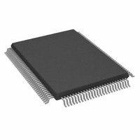
AD9884AKSZ-100 Analog Devices Inc, AD9884AKSZ-100 Datasheet - Page 8

AD9884AKSZ-100
Manufacturer Part Number
AD9884AKSZ-100
Description
100 Msps Graphics Digitizer
Manufacturer
Analog Devices Inc
Datasheet
1.AD9884AKSZ-100.pdf
(24 pages)
Specifications of AD9884AKSZ-100
Display Type
LCD
Interface
Analog
Current - Supply
125mA
Voltage - Supply
3 V ~ 3.6 V
Operating Temperature
-20°C ~ 85°C
Mounting Type
Surface Mount
Package / Case
128-MQFP, 128-PQFP
Lead Free Status / RoHS Status
Lead free / RoHS Compliant
Configuration
-
Digits Or Characters
-
Lead Free Status / RoHS Status
Lead free / RoHS Compliant
Available stocks
Company
Part Number
Manufacturer
Quantity
Price
Company:
Part Number:
AD9884AKSZ-100
Manufacturer:
Analog Devices Inc
Quantity:
10 000
Part Number:
AD9884AKSZ-100
Manufacturer:
ADI/亚德诺
Quantity:
20 000
AD9884A
Pin Name
ANALOG INTERFACE
REFOUT
REFIN
FILT
POWER SUPPLY
V
V
PV
GND
D
DD
D
Function
Internal Reference Output
Output from the internal 1.25 V bandgap reference. This output is intended to drive relatively light loads. It can
drive the AD9884A Reference input directly, but should be externally buffered if it is used to drive other loads as
well. The absolute accuracy of this output is ± 4%, and the temperature coefficient is ± 50 ppm, which is adequate
for most AD9884A applications. If higher accuracy is required, an external reference may be employed. If an exter-
nal reference is used, tie this pin to ground through a 0.1 µF capacitor.
Reference Input
The reference input accepts the master reference voltage for all AD9884A internal circuitry (+1.25 V ± 10%). It
may be driven directly by the REFOUT pin. Its high impedance presents a very light load to the reference source.
This pin should be bypassed to Ground with a 0.1 µF capacitor.
External Filter Connection
For proper operation, the pixel clock generator PLL requires an external filter. Connect the filter shown in Figure
10 to this pin. For optimal performance, minimize noise and parasitics on this node.
Main Power Supply
These pins supply power to the main elements of the circuit. It should be as quiet and filtered as possible.
Digital Output Power Supply
A large number of output pins (up to 52) switching at high speed (up to 140 MHz) generates a lot of power supply
transients (noise). These supply pins are identified separately from the V
minimize output noise transferred into the sensitive analog circuitry. If the AD9884A is interfacing with lower-
voltage logic, V
Clock Generator Power Supply
The most sensitive portion of the AD9884A is the clock generation circuitry. These pins provide power to the
clock PLL and help the user design for optimal performance. The designer should provide “quiet,” noise-free
power to these pins.
Ground
The ground return for all circuitry on chip. It is recommended that the AD9884A be assembled on a single solid
ground plane, with careful attention to ground current paths. See the Design Guide for details.
DD
may be connected to a lower supply voltage (as low as 2.5 V) for compatibility.
PIN FUNCTION DESCRIPTIONS (continued)
–8–
D
pins so special care can be taken to
REV. C


