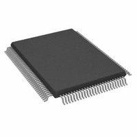
AD9884AKSZ-100 Analog Devices Inc, AD9884AKSZ-100 Datasheet - Page 13

AD9884AKSZ-100
Manufacturer Part Number
AD9884AKSZ-100
Description
100 Msps Graphics Digitizer
Manufacturer
Analog Devices Inc
Datasheet
1.AD9884AKSZ-100.pdf
(24 pages)
Specifications of AD9884AKSZ-100
Display Type
LCD
Interface
Analog
Current - Supply
125mA
Voltage - Supply
3 V ~ 3.6 V
Operating Temperature
-20°C ~ 85°C
Mounting Type
Surface Mount
Package / Case
128-MQFP, 128-PQFP
Lead Free Status / RoHS Status
Lead free / RoHS Compliant
Configuration
-
Digits Or Characters
-
Lead Free Status / RoHS Status
Lead free / RoHS Compliant
Available stocks
Company
Part Number
Manufacturer
Quantity
Price
Company:
Part Number:
AD9884AKSZ-100
Manufacturer:
Analog Devices Inc
Quantity:
10 000
Part Number:
AD9884AKSZ-100
Manufacturer:
ADI/亚德诺
Quantity:
20 000
Writing data to specific control registers of the AD9884A requires
that the 8-bit address of the control register of interest be written
after the slave address has been established. This control register
address is the base address for subsequent write operations. The
base address autoincrements by one for each byte of data written
after the data byte intended for the base address. If more bytes are
transferred than there are available addresses, the address will not
increment and remain at its maximum value of 0Eh. Any base
address higher than 0Eh will not produce an ACKnowledge signal.
Data are read from the control registers of the AD9884A in a
similar manner. Reading requires two data transfer operations:
The base address must be written with the R/W bit of the slave
address byte LOW to set up a sequential read operation.
Reading (the R/W bit of the slave address byte HIGH) begins at
the previously established base address. The address of the read
register autoincrements after each byte is transferred.
To terminate a read/write sequence to the AD9884A, a stop
signal must be sent. A stop signal comprises a LOW-to-HIGH
transition of SDA while SCL is HIGH.
A repeated start signal occurs when the master device driving
the serial interface generates a start signal without first generat-
ing a stop signal to terminate the current communication. This is
used to change the mode of communication (read, write) between
the slave and master without releasing the serial interface lines.
Serial Interface Read/Write Examples
Write to One Control Register
• Start Signal
• Slave Address Byte (R/W Bit = LOW)
• Base Address Byte
• Data Byte to Base Address
• Stop Signal
REV. C
SDA
SCL
SDA
SCL
t
t
STAH
BUFF
BIT 7
t
DHO
BIT 6
Figure 2. Serial Interface—Typical Byte Transfer
Figure 1. Serial Port Read/Write Timing
t
DAL
BIT 5
t
DAH
t
DSU
BIT 4
–13–
BIT 3
Write to Four Consecutive Control Registers
• Start Signal
• Slave Address Byte (R/W Bit = LOW)
• Base Address Byte
• Data Byte to Base Address
• Data Byte to (Base Address + 1)
• Data Byte to (Base Address + 2)
• Data Byte to (Base Address + 3)
• Stop Signal
Read from One Control Register
• Start Signal
• Slave Address Byte (R/W Bit = LOW)
• Base Address Byte
• Start Signal
• Slave Address Byte (R/W Bit = HIGH)
• Data Byte from Base Address
• Stop Signal
Read from Four Consecutive Control Registers
• Start Signal
• Slave Address Byte (R/W Bit = LOW)
• Base Address Byte
• Start Signal
• Slave Address Byte (R/W Bit = HIGH)
• Data Byte from Base Address
• Data Byte from (Base Address + 1)
• Data Byte from (Base Address + 2)
• Data Byte from (Base Address + 3)
• Stop Signal
BIT 2
t
STASU
BIT 1
BIT 0
t
STOSU
ACK
AD9884A


