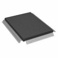
AD9884AKSZ-100 Analog Devices Inc, AD9884AKSZ-100 Datasheet - Page 14

AD9884AKSZ-100
Manufacturer Part Number
AD9884AKSZ-100
Description
100 Msps Graphics Digitizer
Manufacturer
Analog Devices Inc
Datasheet
1.AD9884AKSZ-100.pdf
(24 pages)
Specifications of AD9884AKSZ-100
Display Type
LCD
Interface
Analog
Current - Supply
125mA
Voltage - Supply
3 V ~ 3.6 V
Operating Temperature
-20°C ~ 85°C
Mounting Type
Surface Mount
Package / Case
128-MQFP, 128-PQFP
Lead Free Status / RoHS Status
Lead free / RoHS Compliant
Configuration
-
Digits Or Characters
-
Lead Free Status / RoHS Status
Lead free / RoHS Compliant
Available stocks
Company
Part Number
Manufacturer
Quantity
Price
Company:
Part Number:
AD9884AKSZ-100
Manufacturer:
Analog Devices Inc
Quantity:
10 000
Part Number:
AD9884AKSZ-100
Manufacturer:
ADI/亚德诺
Quantity:
20 000
AD9884A
DESIGN GUIDE
GENERAL DESCRIPTION
The AD9884A is a fully-integrated solution for capturing analog
RGB signals and digitizing them for display on flat panel moni-
tors or projectors. The circuit is also ideal for providing a com-
puter interface for HDTV monitors or as the front-end to high
performance video scan converters.
Implemented in a high performance CMOS process, the inter-
face can capture signals with pixel rates of up to 140 MegaPixels
Per Second (Mpps), and with an Alternate Pixel Sampling mode,
up to 280 Mpps.
800
700
600
500
400
Figure 3. Power Dissipation vs. Frequency
Figure 6. Equivalent Digital Output Circuit
Figure 4. Equivalent Analog Input Circuit
Figure 5. Equivalent Digital Input Circuit
0
20
DIGITAL
G
R
B
INPUT
V
IN
IN
IN
D
V
D
40
FREQUENCY – Mpps
60
355
360
80
100
V
OUTPUT
DIGITAL
D
120
140
160
–14–
The AD9884A includes all necessary input buffering, signal dc
restoration (clamping), offset and gain (brightness and contrast)
adjustment, pixel clock generation, sampling phase control, and
output data formatting. All controls are programmable via a
2-wire serial interface. Full integration of these sensitive analog
functions makes system design straightforward and less sensitive
to the physical and electrical environment.
With a typical power dissipation of only 570 mW and an operat-
ing temperature range of 0°C to 70°C, the device requires no
special environmental considerations.
INPUT SIGNAL HANDLING
Analog Inputs
The AD9884A has three high impedance analog input pins for
the red, green, and blue channels. They will accommodate
signals ranging from 0.5 V to 1.0 V p-p.
Signals are typically brought onto the interface board via a 15-
pin D connector, a VESA P&D connector, a DDWG DVI
connector, or via BNC connectors. The AD9884A should be
located as close as practical to the input connector. Signals
should be routed via matched- impedance traces (normally
75 Ω) to the IC input pins.
At that point the signal should be resistively terminated (75 Ω
to the signal ground return) and capacitively coupled to the
AD9884A inputs through 47 nF capacitors. These capacitors
form part of the dc restoration circuit.
In an ideal world of perfectly matched impedances, the best
performance can be obtained with the widest possible signal
bandwidth. The ultrawide bandwidth inputs of the AD9884A
(500 MHz) can track the input signal continuously as it moves
from one pixel level to the next, and digitize the pixel during a
long, flat pixel time. In many systems, however, there are mis-
matches, reflections, and noise, which can result in excessive
ringing and distortion of the input waveform. This makes it
more difficult to establish a sampling phase that provides good
image quality. It has been shown that a small inductor in series
with the input is effective in rolling off the input bandwidth
slightly, and providing a high quality signal over a wider range of
conditions. Using a Fair-Rite #2508051217Z0 High-Speed
Signal Chip Bead inductor in the circuit of Figure 7 gives good
results in most applications.
HSYNC, VSYNC Inputs
The interface also takes a horizontal sync signal, which is used
to generate the pixel clock and clamp timing. It is possible to
operate the AD9884A without applying HSYNC (using an
external clock, external clamp, and single port output mode) but
a number of features of the chip will be unavailable, so it is
recommended that HSYNC be provided. This can be either a
sync signal directly from the graphics source, or a preprocessed
TTL or CMOS level signal. The HSYNC input includes a
Schmitt trigger buffer for immunity to noise and signals with
long rise times.
Figure 7. Analog Input Interface Circuit
INPUT
RGB
75
47nF
R
G
B
AIN
AIN
AIN
REV. C


